
Intel Celeron Processor on 0.13 Micron Process in the 478-Pin Package Datasheet

Intel
®
Celeron
®
Processor on 0.13 Micron Process in the 478-Pin Package Datasheet 29
Electrical Specifications
2.13 System Bus AC Specifications
The processor system bus timings specified in this section are defined at the processor silicon.
See Chapter 5 for the Celeron processor on 0.13 micron process pin signal definitions.
Table 16 through Table 21 list the AC specifications associated with the processor system bus. All
AGTL+ timings are referenced to GTLREF for both ‘0’ and ‘1’ logic levels unless otherwise
specified.
AGTL+ layout guidelines are available in the appropriate Platform Design Guide (see Table 1).
Care should be taken to read all notes associated with a particular timing parameter.
.
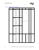
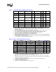
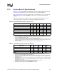
Table 16. System Bus Differential Clock Specifications
T# Parameter Min Nom Max Unit Figure Notes
1
NOTES:
1. Unless otherwise noted, all specifications in this table apply to all processor frequencies.
System Bus Frequency 100 MHz
T1: BCLK[1:0] Period 10.0 10.2 ns 8
2
2. The period specified here is the average period. A given period may vary from this specification as governed
by the period stability specification (T2).
T2: BCLK[1:0] Period Stability 200 ps
3,
4
3. For the clock jitter specification, refer to the CK408 Clock Design Guidelines.
4. In this context, period stability is defined as the worst case timing difference between successive crossover
voltages. In other words, the largest absolute difference between adjacent clock periods must be less than
the period stability.
T3: BCLK[1:0] High Time 3.94 5 6.12 ns 8
T4: BCLK[1:0] Low Time 3.94 5 6.12 ns 8
T5: BCLK[1:0] Rise Time 175 700 ps 8
5
5. Slew rate is measured between the 35% and 65% points of the clock swing (V
L
to V
H
).
T6: BCLK[1:0] Fall Time 175 700 ps 8
5
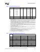
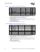
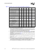
Table 17. System Bus Common Clock AC Specifications
T# Parameter Min Max Unit Figure Notes
1,2,3
NOTES:
1. Unless otherwise noted, all specifications in this table apply to all processor frequencies.
2. Not 100% tested. Specified by design characterization.
3. All common clock AC timings for AGTL+ signals are referenced to the Crossing Voltage (V
CROSS
) of the
BCLK[1:0] at rising edge of BCLK0. All common clock AGTL+ signal timings are referenced at GTLREF at
the processor core.
T10: Common Clock Output Valid Delay 0.12 1.27 ns 10
4
4. Valid delay timings for these signals are specified into the test circuit described in Figure 6 and with GTLREF
at 2/3 VCC ± 2%.
T11: Common Clock Input Setup Time 0.65 ns 10
5
5. Specification is for a minimum swing defined between AGTL+ V
IL_MAX
to V
IH_MIN
. This assumes an edge
rate of 0.4 V/ns to 4.0 V/ns.
T12: Common Clock Input Hold Time 0.40 ns 10
5
T13: RESET# Pulse Width 1 10 ms 11
6,
7,
8
6. RESET# can be asserted asynchronously, but must be deasserted synchronously.
7. This should be measured after VCC and BCLK[1:0] become stable.
8. Maximum specification applies only while PWRGOOD is asserted.