
Intel Celeron D Processor 3xx Sequence

Datasheet 21
Electrical Specifications
2.7 Asynchronous GTL+ Signals
Legacy input signals (such as A20M#, IGNNE#, INIT#, SMI#, SLP#, and STPCLK#) use CMOS
input buffers. All of these signals follow the same DC requirements as GTL+ signals; however, the
outputs are not actively driven high (during a logical 0-to-1 transition) by the processor. These
signals do not have setup or hold time specifications in relation to BCLK[1:0].
All of the Asynchronous GTL+ signals are required to be asserted/de-asserted for at least six
BCLKs for the processor to recognize the proper signal state. See Section 2.11 for the DC
specifications for the Asynchronous GTL+ signal groups. See Section 6.2 for additional timing
requirements for entering and leaving the low power states.
2.8 Test Access Port (TAP) Connection
Due to the voltage levels supported by other components in the Test Access Port (TAP) logic, it is
recommended that the Celeron D processor be first in the TAP chain and followed by any other
components within the system. A translation buffer should be used to connect to the rest of the
chain unless one of the other components is capable of accepting an input of the appropriate
voltage level. Similar considerations must be made for TCK, TMS, TRST#, TDI, and TDO. Two
copies of each signal may be required, with each driving a different voltage level.
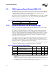
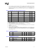
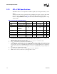
Table 2-4. Signal Characteristics
Signals with R
TT
Signals with no R
TT
A[35:3]#, ADS#, ADSTB[1:0]#, AP[1:0]#, BINIT#,
BNR#, BOOTSELECT
1
, BPRI#, D[63:0]#, DBI[3:0]#,
DBSY#, DEFER#, DP[3:0]#, DRDY#, DSTBN[3:0]#,
DSTBP[3:0]#, HIT#, HITM#, LOCK#, MCERR#,
OPTIMIZED/COMPAT#
1
, PROCHOT#, REQ[4:0]#,
RS[2:0]#, RSP#, TRDY#
NOTES:
1. The OPTIMIZED/COMPAT# and BOOTSELECT pins have a 500–5000 Ω pull-up to V
CCVID
rather than R
TT
.
A20M#, BCLK[1:0], BPM[5:0]#, BR0#, BSEL[1:0],
COMP[1:0], FERR#/PBE#, IERR#, IGNNE#, INIT#,
LINT0/INTR, LINT1/NMI, PWRGOOD, RESET#,
SKTOCC#, SLP#, SMI#, STPCLK#, TDO,
TESTHI[12:0], THERMDA, THERMDC,
THERMTRIP#, VID[5:0], VIDPWRGD,
GTLREF[3:0], TCK, TDI, TRST#, TMS
Open Drain Signals
2
2. Signals that do not have R
TT
, nor are actively driven to their high-voltage level.
BSEL[1:0], VID[5:0], THERMTRIP#, FERR#/PBE#,
IERR#, BPM[5:0]#, BR0#, TDO
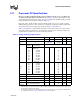
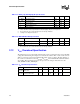
Table 2-5. Signal Reference Voltages
GTLREF V
CC
/2 V
CCVID
/2
BPM[5:0]#, LINT0/INTR, LINT1/NMI, RESET#, BINIT#,
BNR#, HIT#, HITM#, MCERR#, PROCHOT#, BR0#,
A[35:0]#, ADS#, ADSTB[1:0]#, AP[1:0]#, BPRI#, D[63:0]#,
DBI[3:0]#, DBSY#, DEFER#, DP[3:0]#, DRDY#,
DSTBN[3:0]#, DSTBP[3:0]#, LOCK#, REQ[4:0]#, RS[2:0]#,
RSP#, TRDY#
A20M#, IGNNE#, INIT#,
PWRGOOD
1
, SLP#, SMI#,
STPCLK#, TCK
1
, TDI
1
,
TMS
1
, TRST#
1
NOTES:
1. These signals also have hysteresis added to the reference voltage. See Table 2-12 for more information.
VIDPWRGD,
BOOTSELECT,
OPTIMIZED/
COMPAT#