
Intel Celeron D Processor 3xx Sequence

Datasheet 23
Electrical Specifications
2.11 Processor DC Specifications
The processor DC specifications in this section are defined at the processor core silicon and
not at the package pins unless noted otherwise. See Chapter 4 for the pin signal definitions and
signal pin assignments. Most of the signals on the processor FSB are in the GTL+ signal group. The
DC specifications for these signals are listed in Table 2-10.
Previously, legacy signals and Test Access Port (TAP) signals to the processor used low-voltage
CMOS buffer types. However, these interfaces now follow DC specifications similar to GTL+. The
DC specifications for these signal groups are listed in Table 2-11 and Table 2-12.
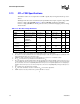
Table 2-8 through Table 2-15 list the DC specifications for the Celeron D processor and are valid
only while meeting specifications for case temperature, clock frequency, and input voltages. Care
should be taken to read all notes associated with each parameter.
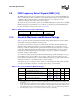
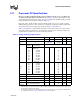
Table 2-8. Voltage and Current Specifications
Symbol Parameter Min Typ Max Unit Notes
VID range VID 1.250 — 1.400 V
1
NOTES:
1. Individual processor VID values may be calibrated during manufacturing such that two devices at the same
speed may have different VID settings.
V
CC
V
CC
See Table 2-9 and
Figure 2-2
VID – I
CC
(max)
* 1.45 mΩ
V
2,3,4
2. These voltages are targets only. A variable voltage source should exist on systems in the event that a differ-
ent voltage is required. See
Section 2.4 and Table 2-2 for more information.
I
CC
Processor
Number
Core Frequency
350
345
340
335
330
325
320
I
CC
for processor with
multiple VID:
3.20 GHz
3.06 GHz
2.93 GHz
2.80 GHz
2.66 GHz
2.53 GHz
2.40 GHz
——
73
73
73
73
73
73
73
A
5
I
SGNT
I
SLP
350
345
340
335
330
325
320
I
CC
Stop-Grant
3.20 GHz
3.06 GHz
2.93 GHz
2.80 GHz
2.66 GHz
2.53 GHz
2.40 GHz
——
40
40
40
40
40
40
40
A
6,7
I
TCC
I
CC
TCC active — — I
CC
A
8
I
CC_VCCA
I
CC
for PLL pins — — 60 mA
9
I
CC_VCCIOPLL
I
CC
for I/O PLL pin — — 60 mA
9
I
CC_GTLREF
I
CC
for GTLREF pins (all pins) — — 200 µA
I
CC_VCCVID
/
VCCVIDLB
I
CC
for VCCVID/VCCVIDLB — — 150 mA
9