
Intel Celeron D Processor 3xx Sequence

24 Datasheet
Electrical Specifications
3. The voltage specification requirements are measured across VCC_SENSE and VSS_SENSE pins at the
socket with a 100 MHz bandwidth oscilloscope, 1.5 pF maximum probe capacitance, and 1 MΩ minimum im-
pedance. The maximum length of ground wire on the probe should be less than 5 mm. Ensure external noise
from the system is not coupled into the oscilloscope probe.
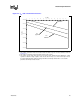
4. Refer to Table 2-9 and Figure 2-2 for the minimum, typical, and maximum V
CC
allowed for a given current. The
processor should not be subjected to any V
CC
and I
CC
combination wherein V
CC
exceeds V
CC_MAX
for a giv-
en current. Moreover, V
CC
should never exceed the VID voltage. Failure to adhere to this specification can
shorten the processor lifetime.
5. I
CC_MAX
is specified at V
CC_MAX
.
6. The current specified is also for AutoHALT state.
7. I
CC
Stop-Grant and I
CC
Sleep are specified at V
CC_MAX
.
8. The maximum instantaneous current the processor will draw while the thermal control circuit is active as in-
dicated by the assertion of PROCHOT# is the same as the maximum I
CC
for the processor.
9. These parameters are based on design characterization and are not tested.
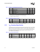
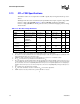
Table 2-9. V
CC
Static and Transient Tolerance
Icc (A)
Voltage Deviation from VID Setting (V)
1,2,3
Maximum Voltage Typical Voltage Minimum Voltage
0 0.000 -0.025 -0.050
5 -0.007 -0.034 -0.060
10 -0.015 -0.042 -0.070
15 -0.022 -0.051 -0.080
20 -0.029 -0.060 -0.090
25 -0.036 -0.068 -0.100
30 -0.044 -0.077 -0.110
35 -0.051 -0.085 -0.120
40 -0.058 -0.094 -0.130
45 -0.065 -0.103 -0.140
50 -0.073 -0.111 -0.150
55 -0.080 -0.120 -0.160
60 -0.087 -0.129 -0.170
65 -0.094 -0.137 -0.180
70 -0.102 -0.146 -0.190
73 -0.106 -0.151 -0.196
NOTES:
1. The loadline specification includes both static and transient limits except for overshoot allowed as
shown in
Section 2.12.
2. This table is intended to aid in reading discrete points on Figure 2-3.
3. The loadlines specify voltage limits at the die measured at the VCC_SENSE and VSS_SENSE
pins. Voltage regulation feedback for voltage regulator circuits must be taken from processor VCC
and VSS pins. Refer to the Voltage Regulator-Down (VRD) 10.0 Design Guidelines for Desktop
Socket 478 for socket loadline guidelines and VR implementation details.