
Intel Celeron D Processor 3xx Sequence

26 Datasheet
Electrical Specifications
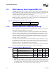
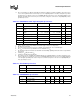
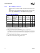
Table 2-10. GTL+ Signal Group DC Specifications
Symbol Parameter Min Max Unit Notes
1
NOTES:
1. Unless otherwise noted, all specifications in this table apply to all processor frequencies.
V
IL
Input Low Voltage 0.0 GTLREF – (0.10 * V
CC
)V
2,3
2. V
IL
is defined as the voltage range at a receiving agent that will be interpreted as a logical low value.
3. The V
CC
referred to in these specifications is the instantaneous V
CC
.
V
IH
Input High Voltage GTLREF + (0.10 * V
CC
)V
CC
V
3,4,5
4. V
IH
is defined as the voltage range at a receiving agent that will be interpreted as a logical high value.
5. V
IH
and V
OH
may experience excursions above V
CC
.
V
OH
Output High Voltage 0.90*V
CC
V
CC
V
3,5
I
OL
Output Low Current N/A
V
CC
/
[0.50*RR
TT_MIN
+R
ON_MIN
]
A
I
LI
Input Leakage Current N/A ± 200 µA
6
6. Leakage to V
SS
with pin held at V
CC
.
I
LO
Output Leakage Current N/A ± 200 µA
7
7. Leakage to V
CC
with pin held at 300 mV.
R
on_compatible
Buffer On Resistance 6.33 10.33 Ω
8
8. These specifications are different depending on whether the platform is forward compatible to the Celeron D proces-
sor or if it is optimized for the Celeron D processor. A compatible platform is one that is designed for a previous gen-
eration processor but has some level of compatibility with the Celeron D processor. An optimized platform is one
designed specifically for the Celeron D processor; however, it may have some level of compatibility with previous
generation processors.
R
on_optimized
Buffer On Resistance 8 12 Ω
8
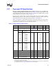
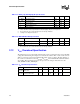
Table 2-11. Asynchronous GTL+ Signal Group DC Specifications
Symbol Parameter Min Max Unit Notes
1
NOTES:
1. Unless otherwise noted, all specifications in this table apply to all processor frequencies.
V
IL
Input Low Voltage 0.0 V
CC
/2 – (0.10 * V
CC
)V
2,3
2. V
IL
is defined as the voltage range at a receiving agent that will be interpreted as a logical low value.
3. LINT0/INTR and LINT1/NMI use GTLREF as a reference voltage. For these two signals
V
IH
= GTLREF + (0.10 * V
CC
) and V
IL
= GTLREF – (0.10 * V
CC
).
V
IH
Input High Voltage V
CC
/2 + (0.10 * V
CC
)V
CC
V
3,4,5,6
4. V
IH
is defined as the voltage range at a receiving agent that will be interpreted as a logical high value.
5. V
IH
and V
OH
may experience excursions above V
CC
.
6. The V
CC
referred to in these specifications refers to instantaneous V
CC
.
V
OH
Output High Voltage 0.90*V
CC
V
CC
V
5,6,7
7. All outputs are open drain.
I
OL
Output Low Current — V
CC
/[0.50*R
TT_MIN
+R
ON_MIN
]A
8
8. The maximum output current is based on maximum current handling capability of the buffer and is not specified into
the test load.
I
IL
Input Leakage Current N/A ± 200 µA
9
9. Leakage to V
SS
with pin held at V
CC
.
I
LO
Output Leakage Current N/A ± 200 µA
10
10. Leakage to V
CC
with pin held at 300 mV.
R
on_compatible
Buffer On Resistance 6.33 10.33 W
11
R
on_optimized
Buffer On Resistance 8 12 W
11