
Intel Celeron D Processor 3xx Sequence


Pin Listing and Signal Descriptions
Datasheet 49
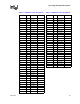
D7 VCC Power/Other
D8 VSS Power/Other
D9 VCC Power/Other
D10 VSS Power/Other
D11 VCC Power/Other
D12 VSS Power/Other
D13 VCC Power/Other
D14 VSS Power/Other
D15 VCC Power/Other
D16 VSS Power/Other
D17 VCC Power/Other
D18 VSS Power/Other
D19 VCC Power/Other
D20 VSS Power/Other
D21 VSS Power/Other
D22 D5# Source Synch Input/Output
D23 D13# Source Synch Input/Output
D24 VSS Power/Other
D25 D15# Source Synch Input/Output
D26 D23# Source Synch Input/Output
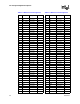
E1 VSS Power/Other
E2 DEFER# Common Clock Input
E3 HITM# Common Clock Input/Output
E4 VSS Power/Other
E5 LINT1 Asynch GTL+ Input
E6 TRST# TAP Input
E7 VSS Power/Other
E8 VCC Power/Other
E9 VSS Power/Other
E10 VCC Power/Other
E11 VSS Power/Other
E12 VCC Power/Other
E13 VSS Power/Other
E14 VCC Power/Other
E15 VSS Power/Other
E16 VCC Power/Other
E17 VSS Power/Other
E18 VCC Power/Other
E19 VSS Power/Other
E20 VCC Power/Other
E21 DBI0# Source Synch Input/Output
Table 4-2. Numerical Pin Assignment
Pin # Pin Name
Signal Buffer
Type
Direction
E22 DSTBN0# Source Synch Input/Output
E23 VSS Power/Other
E24 D17# Source Synch Input/Output
E25 D21# Source Synch Input/Output
E26 VSS Power/Other
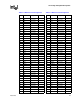
F1 RS0# Common Clock Input
F2 VSS Power/Other
F3 HIT# Common Clock Input/Output
F4 RS2# Common Clock Input
F5 VSS Power/Other
F6 GTLREF Power/Other Input
F7 TMS TAP Input
F8 VSS Power/Other
F9 VCC Power/Other
F10 VSS Power/Other
F11 VCC Power/Other
F12 VSS Power/Other
F13 VCC Power/Other
F14 VSS Power/Other
F15 VCC Power/Other
F16 VSS Power/Other
F17 VCC Power/Other
F18 VSS Power/Other
F19 VCC Power/Other
F20 GTLREF Power/Other Input
F21 DSTBP0# Source Synch Input/Output
F22 VSS Power/Other
F23 D19# Source Synch Input/Output
F24 D20# Source Synch Input/Output
F25 VSS Power/Other
F26 D22# Source Synch Input/Output
G1 ADS# Common Clock Input/Output
G2 BNR# Common Clock Input/Output
G3 VSS Power/Other
G4 LOCK# Common Clock Input/Output
G5 RS1# Common Clock Input
G6 VSS Power/Other
G21 VSS Power/Other
G22 D10# Source Synch Input/Output
G23 D18# Source Synch Input/Output
G24 VSS Power/Other
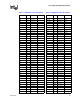
Table 4-2. Numerical Pin Assignment
Pin # Pin Name
Signal Buffer
Type
Direction