
Intel Celeron D Processor 3xx Sequence

Pin Listing and Signal Descriptions
52 Datasheet
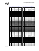
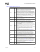
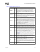
AA7 VSS Power/Other
AA8 VCC Power/Other
AA9 VSS Power/Other
AA10 VCC Power/Other
AA11 VSS Power/Other
AA12 VCC Power/Other
AA13 VSS Power/Other
AA14 VCC Power/Other
AA15 VSS Power/Other
AA16 VCC Power/Other
AA17 VSS Power/Other
AA18 VCC Power/Other
AA19 VSS Power/Other
AA20 TESTHI6 Power/Other Input
AA21 GTLREF Power/Other Input
AA22 D62# Source Synch Input/Output
AA23 VSS Power/Other
AA24 D63# Source Synch Input/Output
AA25 D61# Source Synch Input/Output
AA26 VSS Power/Other
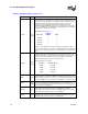
AB1 A35# Source Synch Input/Output
AB2 RSP# Common Clock Input
AB3 VSS Power/Other
AB4 BPM5# Common Clock Input/Output
AB5 BPM1# Common Clock Input/Output
AB6 VSS Power/Other
AB7 VCC Power/Other
AB8 VSS Power/Other
AB9 VCC Power/Other
AB10 VSS Power/Other
AB11 VCC Power/Other
AB12 VSS Power/Other
AB13 VCC Power/Other
AB14 VSS Power/Other
AB15 VCC Power/Other
AB16 VSS Power/Other
AB17 VCC Power/Other
AB18 VSS Power/Other
AB19 VCC Power/Other
AB20 VSS Power/Other
AB21 VSS Power/Other
Table 4-2. Numerical Pin Assignment
Pin # Pin Name
Signal Buffer
Type
Direction
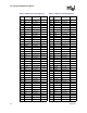
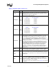
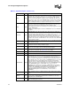
AB22 TESTHI7 Power/Other Input
AB23 PWRGOOD Power/Other Input
AB24 VSS Power/Other
AB25 RESET# Common Clock Input
AB26 SLP# Asynch GTL+ Input
AC1 AP0# Common Clock Input/Output
AC2 VSS Power/Other
AC3 IERR# Asynch GTL+ Output
AC4 BPM2# Common Clock Input/Output
AC5 VSS Power/Other
AC6 BPM0# Common Clock Input/Output
AC7 VSS Power/Other
AC8 VCC Power/Other
AC9 VSS Power/Other
AC10 VCC Power/Other
AC11 VSS Power/Other
AC12 VCC Power/Other
AC13 VSS Power/Other
AC14 VCC Power/Other
AC15 VSS Power/Other
AC16 VCC Power/Other
AC17 VSS Power/Other
AC18 VCC Power/Other
AC19 VSS Power/Other
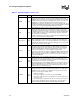
AC20 TESTHI3 Power/Other Input
AC21 TESTHI2 Power/Other Input
AC22 VSS Power/Other
AC23 TESTHI5 Power/Other Input
AC24 TESTHI4 Power/Other Input
AC25 VSS Power/Other
AC26 ITP_CLK0 TAP Input
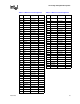
AD1 BOOTSELECT Power/Other Input
AD2 VIDPWRGD Power/Other Input
AD3 VID5 Power/Other Output
AD4 VSS Power/Other
AD5 BSEL1 Power/Other Output
AD6 BSEL0 Power/Other Output
AD7 VCC Power/Other
AD8 VSS Power/Other
AD9 VCC Power/Other
AD10 VSS Power/Other
Table 4-2. Numerical Pin Assignment
Pin # Pin Name
Signal Buffer
Type
Direction