
Document


Electrical Specifications
26 Datasheet
NOTES:
1. Unless otherwise noted, all specifications in this table apply to all processor frequencies.
2. Crossing Voltage is defined as absolute voltage where rising edge of BCLK0 is equal to the falling edge of
BCLK1.
3. Threshold Region is defined as a region entered about the crossing voltage in which the differential receiver
switches. It includes input threshold hysteresis.
4. For Vin between 0 V and V
IH
.
5. Cpad includes die capacitance only. No package parasitics are included.
6. ΔV
CROSS
is defined as the total variation of all crossing voltages as defined in note 2.
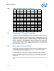
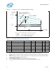
Figure 3. Active V
CC
and I
CC
Loadline Standard Voltage
I
CC
max
V
CC
[V]
V
CC
nom
+/-V
CC
nom * 1.5%
= VR St. Pt. Error 1
/
V
CC, DC
min
V
CC, DC
max
V
CC
max
V
CC
min
10 mV= RIPPLE
I
CC
[A]
0
Slope = -2.1 mV/A at package
VccSense, VssSense pins.
Differential Remote Sense required.
Note 1
/ V
CC
Set Point Error Tolerance is per below:
Tolerance V
CC
Active Mode VID Code Range
--------------- --------------------------------------------------------
+/-1.5% V
CC
> 0.7500 V (VID 0111100).
+/-11.5 mV V
CC
< 0.7500 V (VID 0111100)
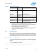
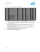
Table 7. FSB Differential BCLK Specifications
Symbol Parameter Min Typ Max Unit Notes
1
V
IH
Input High Voltage 0.660 0.710 0.85 V
V
IL
Input Low Voltage 0 V
V
CROSS
Crossing Voltage 0.25 0.35 0.55 V 2
ΔV
CROSS
Range of Crossing Points 0.14 V 6
V
TH
Threshold Region V
CROSS
- 0.100 V
CROSS
+0.100 V 3
I
LI
Input Leakage Current ±100 µA 4
CPAD Pad Capacitance 0.95 1.2 1.45 pF 5