
Document


Datasheet 27
Electrical Specifications
NOTES:
1. Unless otherwise noted, all specifications in this table apply to all processor frequencies.
2. V
IH
is defined as the minimum voltage level at a receiving agent that interprets as a logical high value.
3. V
IL
is defined as the maximum voltage level at a receiving agent that interprets as a logical low value.
4. V
IH
and V
OH
may experience excursions above V
CCP
. However, input signal drivers must comply with the
signal quality specifications.
5. This is the pull-down driver resistance. Refer to processor I/O Buffer Models for I/V characteristics.
Measured at 0.31*V
CCP
. R
ON
(min) = 0.38*R
TT
.
R
ON
(typ) = 0.45*R
TT
. R
ON
(max) = 0.52*R
TT.
6. GTLREF should be generated from V
CCP
with a 1% tolerance resistor divider. The V
CCP
referred to in these
specifications is the instantaneous V
CCP
.
7. R
TT
is the on-die termination resistance measured at V
OL
of the AGTL+ output driver. Measured at
0.31*V
CCP
. R
TT
is connected to V
CCP
on die. Refer to processor I/O buffer models for I/V characteristics.
8. Specified with on die R
TT
and R
ON
are turned off. Vin between 0 and V
CCP
.
9. Cpad includes die capacitance only. No package parasitics are included.
10. This is the external resistor on the comp pins.
11. On die termination resistance, measured at 0.33*V
CCP
.
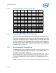
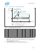
Table 8. AGTL+ Signal Group DC Specifications
Symbol Parameter Min Typ Max Unit Notes
1
V
CCP
I/O Voltage 1.00 1.05 1.10 V
GTLREF Reference Voltage 2/3 V
CCP
V 6
R
COMP
Compensation Resistor 27.23 27.5 27.78 Ω 10
R
ODT
Termination Resistor 55 Ω 11
V
IH
Input High Voltage GTLREF+0.10 V
CCP
V
CCP
+0.10 V 2, 6
V
IL
Input Low Voltage -0.10 0 GTLREF-0.10 V 3, 4
V
OH
Output High Voltage V
CCP
-0.10 V
CCP
V
CCP
6
R
TT
Termination Resistance 50 55 61 Ω 7
R
ON
Buffer On Resistance 22 25 28 Ω 5
I
LI
Input Leakage Current ±100 µA 8
C
PAD
Pad Capacitance 1.6 2.1 2.55 pF 9