
Document


Electrical Specifications
28 Datasheet
NOTES:
1. Unless otherwise noted, all specifications in this table apply to all processor frequencies.
2. The V
CCP
referred to in these specifications refers to instantaneous V
CCP
.
3. Refer to the processor I/O Buffer Models for I/V characteristics.
4. Measured at 0.1*V
CCP
.
5. Measured at 0.9*V
CCP
.
6. For Vin between 0 V and V
CCP
. Measured when the driver is tristated.
7. C
PAD1
includes die capacitance only for DPRSTP#, DPSLP#, PWRGOOD. No package parasitics are included.
8. C
PAD2
includes die capacitance for all other CMOS input signals. No package parasitics are included.
NOTES:
1. Unless otherwise noted, all specifications in this table apply to all processor frequencies.
2. Measured at 0.2 V.
3. V
OH
is determined by value of the external pull-up resistor to V
CCP
. Please refer to platform design guide for
details.
4. For Vin between 0 V and V
OH
.
5. C
PAD
includes die capacitance only. No package parasitics are included.
§
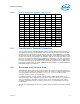
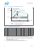
Table 9. CMOS Signal Group DC Specifications
Symbol Parameter Min Typ Max Unit Notes
1
V
CCP
I/O Voltage 1.00 1.05 1.10 V
V
IH
Input High Voltage 0.7*V
CCP
V
CCP
V
CCP
+0.1 V 2
V
IL
Input Low Voltage CMOS -0.10 0.00 0.3*V
CCP
V2, 3
V
OH
Output High Voltage 0.9*V
CCP
V
CCP
V
CCP
+0.1 V 2
V
OL
Output Low Voltage -0.10 0 0.1*V
CCP
V2
I
OH
Output High Current 1.5 4.1 mA 5
I
OL
Output Low Current 1.5 4.1 mA 4
I
LI
Input Leakage Current ±100 µA 6
C
PAD1
Pad Capacitance 1.6 2.1 2.55 pF 7
C
PAD2
Pad Capacitance for CMOS Input 0.95 1.2 1.45 8
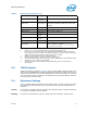
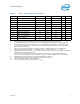
Table 10. Open Drain Signal Group DC Specifications
Symbol Parameter Min Typ Max Unit Notes
1
V
OH
Output High Voltage V
CCP
- 5% V
CCP
V
CCP
+ 5% V 3
V
OL
Output Low Voltage 0 0.20 V
I
OL
Output Low Current 16 50 mA 2
I
LO
Output Leakage Current ±200 µA 4
C
PAD
Pad Capacitance 1.9 2.2 2.45 pF 5