
Document

Datasheet 47
Package Mechanical Specifications and Pin Information
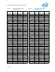
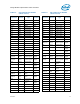
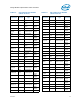
RSVD B2 Reserved
INIT# B3 CMOS Input
LINT1B4CMOS Input
DPSLP# B5 CMOS Input
VSS B6 Power/Other
VCC B7 Power/Other
VSS B8 Power/Other
VCC B9 Power/Other
VCC B10 Power/Other
VSS B11 Power/Other
VCC B12 Power/Other
VSS B13 Power/Other
VCC B14 Power/Other
VCC B15 Power/Other
VSS B16 Power/Other
VCC B17 Power/Other
VCC B18 Power/Other
VSS B19 Power/Other
VCC B20 Power/Other
VSS B21 Power/Other
BSEL[0] B22 CMOS Output
BSEL[1] B23 CMOS Output
VSS B24 Power/Other
THRMDC B25 Power/Other
VCCA B26 Power/Other
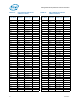
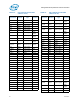
RESET# C1
Common
Clock
Input
VSS C2 Power/Other
RSVD C3 Reserved
IGNNE# C4 CMOS Input
VSS C5 Power/Other
LINT0 C6 CMOS Input
THERMTRIP
#
C7 Open Drain Output
VSS C8 Power/Other
VCC C9 Power/Other
VCC C10 Power/Other
Table 14. Pin Listing by Pin Number
(Sheet 7 of 17)
Pin Name
Pin
Number
Signal Buffer
Type
Direction
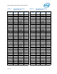
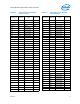
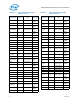
VSS C11 Power/Other
VCC C12 Power/Other
VCC C13 Power/Other
VSS C14 Power/Other
VCC C15 Power/Other
VSS C16 Power/Other
VCC C17 Power/Other
VCC C18 Power/Other
VSS C19 Power/Other
DBR# C20 CMOS Output
BSEL[2] C21 CMOS Output
VSS C22 Power/Other
TEST1 C23 Test
TEST3 C24 Test
VSS C25 Power/Other
VCCA C26 Power/Other
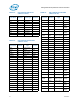
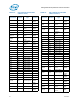
VSS D1 Power/Other
RSVD D2 Reserved
RSVD D3 Reserved
VSS D4 Power/Other
STPCLK# D5 CMOS Input
PWRGOOD D6 CMOS Input
SLP# D7 CMOS Input
VSS D8 Power/Other
VCC D9 Power/Other
VCC D10 Power/Other
VSS D11 Power/Other
VCC D12 Power/Other
VSS D13 Power/Other
VCC D14 Power/Other
VCC D15 Power/Other
VSS D16 Power/Other
VCC D17 Power/Other
VCC D18 Power/Other
VSS D19 Power/Other
IERR# D20 Open Drain Output
Table 14. Pin Listing by Pin Number
(Sheet 8 of 17)
Pin Name
Pin
Number
Signal Buffer
Type
Direction