
Document

Package Mechanical Specifications and Pin Information
48 Datasheet
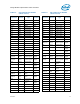
PROCHOT# D21 Open Drain
Input/
Output
RSVD D22 Reserved
VSS D23 Power/Other
DPWR# D24
Common
Clock
Input/
Output
TEST2 D25 Test
VSS D26 Power/Other
DBSY# E1
Common
Clock
Input/
Output
BNR# E2
Common
Clock
Input/
Output
VSS E3 Power/Other
HITM# E4
Common
Clock
Input/
Output
DPRSTP# E5 CMOS Input
VSS E6 Power/Other
VCC E7 Power/Other
VSS E8 Power/Other
VCC E9 Power/Other
VCC E10 Power/Other
VSS E11 Power/Other
VCC E12 Power/Other
VCC E13 Power/Other
VSS E14 Power/Other
VCC E15 Power/Other
VSS E16 Power/Other
VCC E17 Power/Other
VCC E18 Power/Other
VSS E19 Power/Other
VCC E20 Power/Other
VSS E21 Power/Other
D[0]# E22 Source Synch
Input/
Output
D[7]# E23 Source Synch
Input/
Output
VSS E24 Power/Other
D[6]# E25 Source Synch
Input/
Output
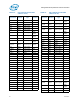
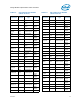
Table 14. Pin Listing by Pin Number
(Sheet 9 of 17)
Pin Name
Pin
Number
Signal Buffer
Type
Direction
D[2]# E26 Source Synch
Input/
Output
BR0# F1
Common
Clock
Input/
Output
VSS F2 Power/Other
RS[0]# F3
Common
Clock
Input
RS[1]# F4
Common
Clock
Input
VSS F5 Power/Other
RSVD F6 Reserved
VCC F7 Power/Other
VSS F8 Power/Other
VCC F9 Power/Other
VCC F10 Power/Other
VSS F11 Power/Other
VCC F12 Power/Other
VSS F13 Power/Other
VCC F14 Power/Other
VCC F15 Power/Other
VSS F16 Power/Other
VCC F17 Power/Other
VCC F18 Power/Other
VSS F19 Power/Other
VCC F20 Power/Other
DRDY# F21
Common
Clock
Input/
Output
VSS F22 Power/Other
D[4]# F23 Source Synch
Input/
Output
D[1]# F24 Source Synch
Input/
Output
VSS F25 Power/Other
D[13]# F26 Source Synch
Input/
Output
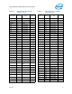
VSS G1 Power/Other
TRDY# G2
Common
Clock
Input
RS[2]# G3
Common
Clock
Input
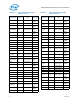
Table 14. Pin Listing by Pin Number
(Sheet 10 of 17)
Pin Name
Pin
Number
Signal Buffer
Type
Direction