
Personal Computer User Manual


Intel
®
820E Chipset
R
Design Guide 13
1. Introduction
The Intel
®
820E Chipset Design Guide provides design recommendations for systems using the Intel
®
820E chipset. This includes motherboard layout, routing guidelines, system design issues, system
requirements, debug recommendations, and board schematics. In addition to providing motherboard
design recommendations (e.g., layout and routing guidelines), this document also addresses system
design issues such as thermal requirements for Intel 820E chipset-based systems. The design
recommendations should be used during system design. The guidelines have been developed to provide
maximum flexibility to board designers while reducing the risk of board-related issues.
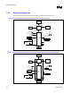
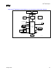
The Intel board schematics in Appendix A: Reference Design Schematics (Uniprocessor) implement
Intel
®
PGA370 architecture and are intended for use as references by board designers. While the
schematics included cover specific designs, the core schematics for each chipset component remain the
same for most Intel 820E chipset platforms. The appendix provides a set of reference schematics for each
chipset component, in addition to common motherboard options. Additional flexibility is possible via
other permutations of these options and components.
1.1. About This Design Guide
This design guide is intended for hardware designers who are experienced with PC architectures and
board design. This design guide assumes that the designer has a working knowledge of the vocabulary
and practices of PC hardware design.
• Chapter 1, Introduction — This chapter introduces the designer to the purpose and organization of
this design guide, and provides a list of references of related documents. This chapter also provides
an overview of the Intel 820E chipset.
• Chapter 2, Layout/Routing Guidelines — This chapter provides a detailed set of motherboard
layout and routing guidelines for designing an Intel 820E chipset-based platform. The
motherboard’s functional units are discussed (e.g., chipset component placement, system bus
routing, system memory layout, display cache interface, hub interface, IDE, AC’97, USB, interrupts,
SMBUS, PCD, LPC/FWH Flash BIOS, and RTC).
• Chapter 4, Advanced System Bus Design — This chapter discusses the AGTL+ guidelines and
theory of operation. It also provides more details about the methodologies used to develop these
guidelines.
• Chapter 4, Clocking — This chapter provides the motherboard clocking guidelines (e.g., clock
architecture, routing, capacitor sites, clock power decoupling, and clock skew).
• Chapter 5, System Manufacturing — This chapter includes the board stack-up requirements.
• Chapter 6, System Design Considerations— This chapter includes the guidelines for power
delivery, decoupling, thermal, and power sequencing.
• Appendix A, Reference Design Schematics (Uniprocessor) — This appendix provides a set of
schematics for uniprocessor designs. It also provides a feature list for board design.