
Personal Computer User Manual

Intel
®
820E Chipset
R
Design Guide 169
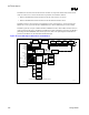
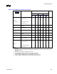
4.2.3. MCH to DRCG
• PclkM
• PclkN
• VddIPD
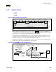
Figure 89. MCH-to-DRCG Routing Diagram
Ground
Ground/Power Plane
6 mils
4.5 mils
1.4 mils
1.4 mils
6 mils
VddiPD
6 mils
6 mils
Ground
6 mils
6 mils
Hclkout
6 mils
6 mils
Rclkout
6 mils
6 mils
Ground
6 mils
mch_drcg_route
Hclkout, Rclkout, and VddIPD should be routed as shown in Figure 89. Note that the VddIPD pin can be
connected directly to 1.8 V near the DRCG, if the 1.8 V plane extends near the DRCG. However, if a 1.8
V trace must be run, it should originate at the MCH and be routed as shown.
The maximum length for Hclkout and Rclkout is 6 inches. Additionally, Hclkout and Rclkout must be
length-matched (to each other) within 50 mils. These signals should be routed on the same layer. If the
signals must switch layers, then
both signals should change layers together.
If VddIPD is connected to the 1.8 V plane using a via (e.g., if a trace is not run from the MCH), Hclkout
and Rclkout must still be routed differentially and ground-isolated.
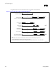
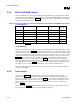
Figure 90. Direct RDRAM* Clock Routing Dimensions
rambus_clk_rout
e
MCH
RIMM_0 RIMM_1
A B C
0"-3.50"
0.4"-0.45"
0"-3"
DRCG
D
(A)
=
CTM/CTM#
RIMM
t
o
MCH
(A) = CFM/CFM# MCH to RIMM
(B) = RIMM to RIMM for Clocks
(C) = RIMM to Termination
(D) = DRCG to RIMM
CFM/CFM#
CTM/CTM#
0"-6"
Term