
Personal Computer User Manual

Intel
®
820E Chipset
R
Design Guide 53
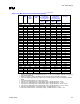
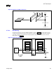
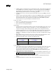
Table 8. Line Matching and Via Compensation Example
1,2,3,4,5,6,7,8,9,10
Signal Ball on
MCH
Nominal
RSL
Length
(mils)
Package
Dimension
(mils)
Motherboard Trace
Length When
Routed on Bottom
(i.e., Real Via)
Motherboard Trace
Length When
Routed on Top
(i.e., Dummy Via)
Recommended
Routing
Min.
(mils)
Max.
(mils)
Min.
(mils)
Max.
(mils)
Formula A Formula B
DQA0 A13 2000 138.14 1851.86 1871.86 1876.86 1896.86 Top
DQA1 C13 2000 19.11 1970.89 1990.89 1995.89 2015.89 Bottom
DQA2 A14 2000 163.16 1826.84 1846.84 1851.84 1871.84 Top
DQA3 C14 2000 39.87 1950.13 1970.13 1975.13 1995.13 Bottom
DQA4 B14 2000 97.54 1892.46 1912.46 1917.46 1937.46 Top
DQA5 C15 2000 62.67 1927.33 1947.33 1952.33 1972.33 Bottom
DQA6 A15 2000 186.11 1803.90 1823.90 1828.90 1848.90 Top
DQA7 C16 2000 95.70 1894.30 1914.30 1919.30 1939.30 Bottom
DQA8 A16 2000 230.20 1759.81 1779.81 1784.81 1804.81 Top
DQB0 C7 2000 39.56 1950.44 1970.44 1975.44 1995.44 Bottom
DQB1 B7 2000 95.83 1894.17 1914.17 1919.17 1939.17 Top
DQB2 C6 2000 63.49 1926.51 1946.51 1951.51 1971.51 Bottom
DQB3 A6 2000 153.69 1836.31 1856.31 1861.31 1881.31 Top
DQB4 C5 2000 97.33 1892.67 1912.67 1917.67 1937.67 Bottom
DQB5 A5 2000 191.43 1798.57 1818.57 1823.57 1843.57 Top
DQB6 B5 2000 152.47 1837.53 1857.53 1862.53 1882.53 Bottom
DQB7 A4 2000 237.71 1752.29 1772.29 1777.29 1797.29 Top
DQB8 C4 2000 138.29 1851.71 1871.71 1876.71 1896.71 Bottom
RQ0 A7 2000 179.49 1810.51 1830.51 1835.51 1855.51 Top
RQ1 C8 2000 27.12 1962.88 1982.88 1987.88 2007.88 Bottom
RQ2 A8 2000 162.21 1827.79 1847.79 1852.79 1872.79 Top
RQ3 C9 2000 5.80 1984.20 2004.20 2009.20 2029.20 Bottom
RQ4 B9 2000 71.70 1918.30 1938.30 1943.30 1963.30 Top
RQ5 A9 2000 133.88 1856.12 1876.12 1881.12 1901.12 Bottom
RQ6 A10 2000 122.20 1867.81 1887.81 1892.81 1912.81 Top
RQ7 C10 2000 0.00 1990.00 2010.00 2015.00 2035.00 Bottom
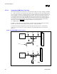
FORMULA C FORMULA D
CFM A12 2000 132.37 1906.85 1932.37 Bottom
CFM# B12 2000 64.63 1976.02 2001.54 Bottom
CTM B11 2000 56.06 1984.76 2010.29 Top
CTM# A11 2000 126.34 1913.01 1938.53 Top
NOTES:
1. Signals connecting to side A of the RIMM connector (i.e., A1, A2, A3, etc.) should be routed on the top (primary
side) of the motherboard.
2. Signals connecting to side B of the RIMM connector should be routed on the bottom (solder side).
3. These trace lengths apply only from the MCH to the first RIMM. All signals must match exactly from RIMM to
RIMM.
4. Clock trace lengths include the 1.021 trace velocity factor.
5. Formula A min.: Motherboard trace = (Nominal RSL length – package dimension) – 10 mils
6. Formula A max.: Motherboard trace = (Nominal RSL length – package dimension) + 10 mils
7. Formula B min.: Motherboard trace = (Nominal RSL length – package dimension) – 10 mils + 25 mil
8. Formula B max.: Motherboard trace = (Nominal RSL length – package dimension) + 10 mils + 25 mils
9. Formula C: Motherboard trace = (Nominal RSL length – package dimension) × 1.021
10. Formula D: Motherboard trace = (Nominal RSL length – package dimension + 25 mils) × 1.021