Intel® Itanium® Processor 9300 Series and 9500 Series Intel® Intel® Intel® Intel® Intel® Itanium® Itanium® Itanium® Itanium® Itanium® Processor Processor Processor Processor Processor Quad-Core 1.86-1.73 GHz Quad-Core 1.73-1.60 GHz Quad-Core 1.60-1.46 GHz Quad-Core 1.46-1.33 GHz Dual-Core 1.60 GHz Fixed Intel® Intel® Intel® Intel® Itanium® Itanium® Itanium® Itanium® Processor Processor Processor Processor Eight-Core 2.53 GHz with 32 MB LLC Cache 9560 Four-Core 2.
INFORMATION IN THIS DOCUMENT IS PROVIDED IN CONNECTION WITH INTEL PRODUCTS. NO LICENSE, EXPRESS OR IMPLIED, BY ESTOPPEL OR OTHERWISE, TO ANY INTELLECTUAL PROPERTY RIGHTS IS GRANTED BY THIS DOCUMENT.
Contents 1 Introduction .............................................................................................................. 9 1.1 Overview ........................................................................................................... 9 1.2 Architectural Overview ....................................................................................... 15 1.2.1 Intel® Itanium® Processor 9300 Series Overview ....................................... 15 1.2.
2.14 Test Access Port (TAP) Connection .......................................................................71 3 Pin Listing................................................................................................................73 3.1 Processor Package Bottom Pin Assignments...........................................................73 3.1.1 Package Bottom Pin Listing by Pin Name ....................................................73 3.1.2 Pin Listing by Pin Number ..............................
Figures 1-1 1-2 1-3 2-1 2-2 2-3 2-4 2-5 2-6 2-7 2-8 2-9 2-10 2-11 2-12 2-13 2-14 2-15 2-16 2-17 2-18 2-19 2-20 4-1 4-2 4-3 4-4 4-5 4-6 4-7 4-8 4-9 4-10 5-1 5-2 6-1 Intel® Itanium® Processor 9300 Series Processor Block Diagram ............................. 16 Intel® Itanium® Processor 9500 Series Processor Block Diagram ............................. 17 Intel® Itanium® Processor 9500 Series Firmware Diagram...................................... 18 Active ODT for a Differential Link Example ..................
Tables 1-1 2-1 2-2 2-3 2-4 2-5 2-6 2-7 2-8 2-9 2-10 2-11 2-12 2-13 2-14 2-15 2-16 2-17 2-18 2-19 2-20 2-21 2-22 2-23 2-24 2-25 2-26 2-27 2-28 2-29 2-30 2-31 2-32 6 Intel® Itanium® Processor 9300 Series and Intel® Itanium® Processor 9500 Series Feature Comparison....................................19 Signals with RTT ................................................................................................24 Signal Groups .............................................................................
2-33 2-34 2-35 2-36 2-37 2-38 2-39 2-40 3-1 3-2 3-3 3-4 3-5 3-6 3-7 3-8 3-9 3-10 4-1 4-2 4-3 4-4 4-5 5-1 5-2 5-3 5-4 5-5 6-1 6-2 6-3 6-4 6-5 7-1 SMBus and Serial Presence Detect (SPD) Bus Signal Group DC Specifications ............ 55 Debug Signal Group DC Specifications.................................................................. 56 PIROM Signal Group DC Specifications .................................................................
Revision History Document Number Revision Number 322821 -002 • Initial release of the 9300/9500 document. 322821 -001 • Initial release of the document.
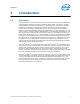
Introduction 1 Introduction 1.1 Overview The Intel® Itanium® Processor 9300 Series and Intel® Itanium® Processor 9500 Series employ Explicitly Parallel Instruction Computing (EPIC) design concepts for a tighter coupling between hardware and software. In this design style, the interface between hardware and software is designed to enable the software to exploit all available compile-time information, and efficiently deliver this information to the hardware.
Introduction 10 Intel® Itanium® Processor 9300 Series and 9500 Series Datasheet
Introduction Intel® Itanium® Processor 9300 Series Intel® Intel® Intel® Intel® Intel® Itanium® Itanium® Itanium® Itanium® Itanium® Processor Processor Processor Processor Processor Quad-Core 1.86-1.73 GHz Quad-Core 1.73-1.60 GHz Quad-Core 1.60-1.46 GHz Quad-Core 1.46-1.33 GHz Dual-Core 1.
Introduction The Intel® Itanium® Processor 9300 Series delivers new levels of flexibility, reliability, performance, and cost-effective scalability for your most data-intensive business and technical applications. It provides 24 megabytes L3 cache accessed at core speed, Hyper-Threading Technology for increased performance, Intel® Virtualization Technology for improved virtualization, Intel® Cache Safe Technology for increased availability.
Introduction Intel® Itanium® Processor 9500 Series Intel® Intel® Intel® Intel® Itanium® Itanium® Itanium® Itanium® Processor Processor Processor Processor Eight-Core 2.53 GHz with 32 MB LLC Cache 9560 Four-Core 2.40 GHz with 32 MB LLC Cache 9550 Eight-Core 2.13 GHz with 24 MB LLC Cache 9540 Four-Core 1.73 GHz with 20 MB LLC Cache 9520 Product Features — Intel® Turbo Boost Technology, featuring sustained boost. — Architected firmware stack, including PAL and SAL support.
Introduction The Intel® Itanium® Processor 9500 Series delivers increased levels of flexibility, reliability, performance, and cost-effective scalability for your most data-intensive business and technical applications. The Intel® Itanium® Processor 9500 Series processor provides up to 32 megabytes LLC cache, Hyper-Threading Technology for increased performance, Intel® Virtualization Technology for improved virtualization, Intel® Cache Safe Technology for increased availability.
Introduction replay can be initiated for any instruction in the pipeline that encounters a resource hazard, a copy of each instruction is maintained in the instruction buffer until the instruction has successfully traversed the pipeline and is no longer needed. If necessary, an instruction can replay multiple times. As a result, Intel® Instruction Replay Technology automatically detects and many corrects soft errors in the instruction pipeline.
Introduction Figure 1-1. Intel® SMI Intel® SMI 1.2.
Introduction Figure 1-2. Intel® Itanium® Processor 9500 Series Processor Block Diagram The Intel QPI viral and poison fields are used to flag corrupted system state and bad data accordingly. Once it has “gone viral”, an Intel QPI agent will set the viral field within all packet headers. Viral mode is entered in three ways: receiving a viral packet, upon a detecting fatal/panic error, or when a global viral signal (from Cboxes) is asserted. Viral is cleared on Reset.
Introduction Protection Keys provide a method to restrict permission by tagging each virtual page with a unique protection domain identifier. The Protection Key Registers (PKR) represent a register cache of all protection keys required by a process. The operating system is responsible for management and replacement polices of the protection key cache. Before a memory access (including IA-32) is permitted, the processor compares a translation’s key value against all keys contained in the PKRs.
Introduction 1.3 Processor Feature Comparison The Intel® Itanium® Processor 9300 Series processor and Intel® Itanium® Processor 9500 Series processor features are compared below in Table 1-1. Intel® Itanium® Processor 9300 Series and Intel® Itanium® Processor 9500 Series Feature Comparison Table 1-1. Description Socket Transistors Intel® Itanium® Processor 9300 Series Intel® Itanium® Processor 9500 Series LG1248 LG1248 2 billion 3.1 billion up to 4/8 up to 8/16 up to 1.
Introduction Intel® Itanium® Processor 9300 Series Intel® Itanium® Processor 9500 Series Memory patrolling Supported Supported Memory migration Supported Supported Not Supported Supported Supported Supported Description Support for mixing of x4 and x8 on the same DDR channel Online/Offline CPU (OS assisted) Online/Offline Memory (OS assisted) Supported Supported Online/Offline I/O Hub Supported Supported 130W, 155W, 185W 130W and 170W Thermal Design Power (TDP) SKUs Notes: 1.
Introduction address or data), the ‘_N’ notation implies that the signal is inverted. For example, D[3:0] = ‘HLHL’ refers to a Hex ‘A’, and D [3:0] _N = ‘LHLH’ also refers to a Hex ‘A’ (H = High logic level, L = Low logic level). A signal name has all capitalized letters, for example, VCTERM. A symbol referring to a voltage level, current level, or a time value carries a plain subscript, for example, Vccio, or a capitalized abbreviated subscript, for example, TCO. 1.
Introduction 22 Intel® Itanium® Processor 9300 Series and 9500 Series Datasheet
Electrical Specifications 2 Electrical Specifications This chapter describes the electrical specifications of the Intel® Itanium® Processor 9300 Series and 9500 Series processors. 2.1 Intel® QuickPath Interconnect and Intel® Scalable Memory Interconnect Differential Signaling The links for Intel® QuickPath Interconnect (Intel® QPI) and Intel® Scalable Memory Interconnect (Intel® SMI) signals use differential signaling. The Intel® SMI bus pins are referred to as FB-DIMM pins on the package.
Electrical Specifications Table 2-1. Signals with RTT Signal 2.
Electrical Specifications Table 2-2.
Electrical Specifications Table 2-2.
Electrical Specifications Table 2-3. Symbol Intel® QuickPath Interconnect/Intel® Scalable Memory Interconnect Reference Clock Specifications (Sheet 2 of 2) Parameter TStable Allowed time before ringback TREFCLK-JITTER-RMS- Accumulated rms jitter over n UI of a given PLL model output in response to the jittery reference clock input. The PLL output is generated by convolving the measured reference clock phase jitter with a given PLL transfer function. Here n=12.
Electrical Specifications Figure 2-4. Differential Edge Rate Definition ERRefclk-diff-Rise ERRefclk-diff-Fall VRefclk-diff-ih = 150 mV 0.0 V VRefclk-diff-il = –150 mV REFCLKdiff Figure 2-5. VRB and TStable Definitions TStable VRefclk-diff-ih = 150 mV VRB- diff max 100 mV 0.0 V VRB-diff min =–100 mV VRefclk-diff-ih =– 150 mV REFCLK diff 2.4 TStable Intel® QuickPath Interconnect and Intel® SMI Signaling Specifications . 2.4.
Electrical Specifications Table 2-4. Intel® Itanium® Processor 9300 Series Clock Frequency Table Intel® QuickPath Interconnect Forwarded Clock Frequency Intel® QuickPath Interconnect Data Transfer Rate 33.33 MHz 66.66 MT/s (see note 1) 2.40 GHz 4.8 GT/s Notes: 1. This speed is the 1/4 SysClk Frequency. Table 2-5. Intel® Itanium® Processor 9300 Series Transmitter Parameter Values for Intel® QuickPath Interconnect and Intel SMI Channels @ 4.
Electrical Specifications Table 2-5. Intel® Itanium® Processor 9300 Series Transmitter Parameter Values for Intel® QuickPath Interconnect and Intel SMI Channels @ 4.8 GT/s (Sheet 2 of 2) Symbol Parameter Min TXDUTY-CYCLE-PIN Transmitter clock or data duty cycle at the pin. Transmit duty cycle at the pin, defined as UI to UI jitter as specified by the Intel® QPI Electrical Specification, Rev 1.0. TTX-DATA-CLK-SKEW-PIN Nom Max Units Notes -0.076 0.
Electrical Specifications Table 2-6. Intel® Itanium® Processor 9300 Series Receiver Parameter Values for Intel® QuickPath Interconnect and Intel® SMI Channels @ 4.8 GT (Sheet 2 of 2) Symbol Parameter Min Nom Max 0.6 Units Notes UI 4 TRX-eye-pin Minimum eye width at pin for clk and data QPI BERLane Bit Error Rate per lane valid for 4.8 and 6.4 GT/s 1.0E-14 Events SMI BERLane Bit Error Rate per lane valid for 4.8 and 6.4 GT/s 1.0E-12 Events Notes: 1.
Electrical Specifications Figure 2-7. TX Return Loss Figure 2-8. RX Return Loss 2.4.2 Intel® Itanium® Processor 9500 Series Requirements for Intel® QuickPath Interconnect for 4.8 and 6.4 GT/s The applicability of this section applies to Intel® Itanium® Processor 9500 Series. This section contains information for slow boot up speed (1/4 frequency of the reference clock), 4.8 GT/s, and 6.4 GT/s, for Intel® QPI and Intel® SMI.
Electrical Specifications The transfer rates available for the processor are shown in Table 2-7. Transmitter and receiver parameters for Intel® QPI slow mode, Intel® QPI and Intel® SMI are shown in Table 2-8 and Table 2-9 respectively. Table 2-7. Intel® Itanium® Processor 9500 Series Clock Frequency Table Intel® QuickPath Interconnect Forwarded Clock Frequency Intel® QuickPath Interconnect Data Transfer Rate 33.33 MHz 66.66 MT/s (see note 1) 2.40 GHz 4.8 GT/s 3.2 GHz 6.4 GT/s Notes: 1.
Electrical Specifications Table 2-8. Intel® Itanium® Processor 9500 Series Link Speed Independent Specifications (Sheet 2 of 2) Symbol Parameter ZTX_LINK_DETECT Link Detection Resistor VTX_LINK_DETECT Min Nom 500 Max Unit 2000 Ω Link Detection Resistor Pull-up Voltage max VCCIO V TDATA_TERM_SKEW Skew between first to last data termination meeting ZRX_LOW_CM_DC 128 UI TINBAND_RESET_ SENSE Time taken by inband reset detector to sense Inband Reset 1.
Electrical Specifications Table 2-9. Intel® Itanium® Processor 9500 Series Transmitter and Receiver Parameter Values for Intel® QPI Channel at 4.8 GT/s (Sheet 2 of 2) Symbol Parameter Min Nom TXclk-acc-jit-N_UI-1E-7 p-p accumulated jitter out of transmitter over 0 <= n <= N UI where N=12, measured with 1E-7 probability. 0 0.15 UI TXclk-acc-jit-N_UI-1E-9 p-p accumulated jitter out of transmitter over 0 <= n <= N UI where N=12, measured with 1E-9 probability. 0 0.
Electrical Specifications Table 2-10. Intel® Itanium® Processor 9500 Series Transmitter and Receiver Parameter Values for Intel® QPI at 6.4 GT/s (Sheet 2 of 2) Symbol Parameter Min VTx-cm-ac-pin Transmitter output AC common mode, defined as ((VD+ + VD-)/2 VTx-cm-dc-pin) -0.0375 Nom Max 0.0375 Unit 2 Fraction of VTx-diff-pp-pin TXduty-pin Average of absolute UI-UI jitter -0.06 0.06 UI TXjitUI-UI-1E-7-pin UI-UI jitter measured at Tx output pins with 1E-7 probability. -0.085 0.
Electrical Specifications 2.4.3 Intel® Itanium® Processor 9500 Series Processor Requirements for Intel® SMI Specifications for 6.4 GT/s This section defines the high-speed differential point-to-point signaling link for Intel® SMI for the Intel® Itanium® Processor 9500 Series. The link consists of a transmitter and a receiver and the interconnect between them. The specifications described in this section covers 6.4 Gb/s operation. The parameters for Intel® SMI at 6.
Electrical Specifications Table 2-11. Intel® Itanium® Processor 9500 Series Transmitter and Receiver Parameter Values for Intel® SMI at 6.4 GT/s and lower (Sheet 2 of 2) Symbol VRx-Vmargin Parameter Min Nom Any data lane Rx input voltage (differential pp) measured at BER=1E-9 Max 100 Unit mV Timing width for any data lane using repetitive patterns and clean forwarded CLK, measured at BER=1E-9 0.
Electrical Specifications At conditions exceeding absolute maximum and minimum ratings, neither functionality nor long-term reliability can be expected. Moreover, if a device is subjected to these conditions for any length of time, then, when returned to conditions within the functional operating condition limits, it will either not function, or its reliability will be severely degraded.
Electrical Specifications • Unless otherwise noted, all specifications in the tables apply to all frequencies • For the Intel® Itanium® Processor 9300 Series and Intel® Itanium® Processor 9500 Series, these specifications are based on characterized data from silicon measurements. 2.6.1 Flexible Motherboard Guidelines for the Intel® Itanium® Processor 9300 Series The Flexible Motherboard (FMB) guidelines are estimates of the maximum ratings that the processor will have over certain time periods.
Electrical Specifications 2. These voltages are target only. A variable voltage source should exist on systems in the event that a different voltage is required. See Ararat Voltage Regulator Module Design Guide for more information. 3. Uncore, Core, and Cache voltage and Current Rating are at the Package Pad. 4. The voltage specification requirements are measured across the VCCCORESENSE and VSSCORESENSE pins using an oscilloscope set to a 100 MHz bandwidth and probes that are 1.
Electrical Specifications Table 2-17.
Electrical Specifications 2.6.2 Flexible Motherboard Guidelines for the Intel® Itanium® Processor 9500 Series The Flexible Motherboard (FMB) guidelines are estimates of the maximum ratings that the processor will have over certain time periods. The ratings are only estimates as actual specifications for future processors may differ. The processor may or may not have specifications equal to the FMB value in the foreseeable future.
Electrical Specifications 7. The FMB remote sense tolerance is ±2.5% for DC to 20 MHz at the package, where ±1.5% is allotted for a DC to 1 MHz range and an additional ±1.0% for 1 MHz to 20 MHz. Similarly, ±6.4% is allotted for DC to 20 MHz at the die. It is expected that VCCIO regulators meet ±1.5% at the remote sense location based on the general remote sense termination point location as described in Figure 2-16 VR Sense Point (Representation).
Electrical Specifications Table 2-20. VCCUNCORE Static and Transient Tolerance for Intel® Itanium® Processor 9300 Series Uncore Current (A) Voltage Deviation from VID Setting (V)1,2,3,4 V CC_Max VCC_Typ VCC_Min 0 VID - 0 VID - 0.02 VID - 0.04 5 VID - 0.02 VID - 0.04 VID - 0.06 10 VID - 0.04 VID - 0.06 VID - 0.08 15 VID - 0.06 VID - 0.08 VID - 0.1 20 VID - 0.08 VID - 0.1 VID - 0.12 25 VID - 0.1 VID - 0.12 VID - 0.14 30 VID - 0.12 VID - 0.14 VID - 0.16 35 VID - 0.14 VID - 0.
Electrical Specifications 2.6.3.2 Core Static and Transient Tolerances Table 2-21 and Figure 2-11 specify static and transient tolerances for the core outputs. Table 2-21. VCCCORE Static and Transient Tolerance for Intel® Itanium® Processor 9300 Series (Sheet 1 of 2) Core Current (A) 46 Voltage Deviation from VID Setting (V)1,2,3,4 ICC_CORE V CC_Max VCC_Typ VCC_Min 0 VID - 0 VID - 0.02 VID - 0.04 5 VID - 0.004 VID - 0.024 VID - 0.044 10 VID - 0.009 VID - 0.029 VID - 0.049 15 VID - 0.
Electrical Specifications Table 2-21. VCCCORE Static and Transient Tolerance for Intel® Itanium® Processor 9300 Series (Sheet 2 of 2) Core Current (A) Voltage Deviation from VID Setting (V)1,2,3,4 ICC_CORE V CC_Max VCC_Typ VCC_Min 170 VID - 0.145 VID - 0.165 VID - 0.185 175 VID - 0.149 VID - 0.169 VID - 0.189 180 Notes: 1. 2. 3. 4. The VCC_MIN and VCC_MAX load lines represent static and transient limits. This table is intended to aid in reading discrete points on Figure 2-11.
Electrical Specifications Table 2-22. VCCCACHE Static and Transient Tolerance for Intel® Itanium® Processor 9300 Series Cache Current (A) Voltage Deviation from VID Setting (V)1,2,3,4 V CC_Max ICC_CACHE VCC_Typ VCC_Min 0 VID - 0 VID - 0.02 VID - 0.04 5 VID - 0.017 VID - 0.037 VID - 0.057 10 VID - 0.035 VID - 0.055 VID - 0.075 15 VID - 0.052 VID - 0.072 VID - 0.092 20 VID - 0.069 VID - 0.089 VID - 0.109 25 VID - 0l.086 VID - 0.106 VID - 0.126 30 VID - 0.104 VID - 0.
Electrical Specifications 2.6.4 Intel® Itanium® Processor 9500 Series Uncore and Core Tolerances 2.6.4.1 Uncore Static and Transient Tolerances Table 2-23 and Figure 2-13 specify static and transient tolerances for the uncore outputs. Table 2-23. VCCUNCORE Static and Transient Tolerance for the Intel® Itanium® Processor 9500 Series Uncore Current (A) ICC_UNCORE Voltage Deviation from VID Setting (V)1,2,3,4 V CC_Max VCC_Typ VCC_Min 0 VID + 0.015 VID VID - 0.015 5 VID + 0.00875 VID - 0.
Electrical Specifications Figure 2-13. VCCUNCORE Static and Transient Tolerance for the Intel® Itanium® Processor 9500 Series VccUnCore Tolerance Band 0.0150 VccUnCore ACMax (V) Normalized VccUnCore (V) -0.0050 VccUnCore DCMax (V) Normalized VccUnCore (V) -0.0250 VccUnCore DCMin (V) -0.0450 VccUnCore ACMin (V) -0.0650 -0.0850 -0.1050 -0.1250 -0.1450 -0.1650 0 20 40 60 80 100 120 IccUnCore (A) Figure 2-14.
Electrical Specifications Table 2-24. VCCCORE Static and Transient Tolerance for the Intel® Itanium® Processor 9500 Series Core Current (A) Voltage Deviation from VID Setting (V)1,2,3,4 ICC_CORE V CC_Max 0 5 VCC_Typ VCC_Min VID + 0.015 VID VID - 0.015 VID + 0.005 VID - 0.010 VID - 0.025 10 VID - 0.005 VID - 0.020 VID - 0.035 15 VID - 0.015 VID - 0.030 VID - 0.045 20 VID - 0.025 VID - 0.040 VID - 0.055 25 VID - 0.035 VID - 0.050 VID - 0.065 30 VID - 0.045 VID - 0.060 VID - 0.
Electrical Specifications 2.6.5 Overshoot and Undershoot Guidelines Overshoot (or undershoot) is the value of the maximum voltage above or below VSS. The overshoot and undershoot specifications limit transitions beyond VCCIO or VSS due to the fast signal edge rates. The processor can be damaged by single and/or repeated overshoot or undershoot events on any input, output, or I/O buffer if the charge is large enough (that is, if the overshoot or undershoot is great enough).
Electrical Specifications Table 2-25. Overshoot and Undershoot Specifications For Differential Intel® QuickPath Interconnect and Intel® SMI and Single-Ended Signals for the Intel® Itanium® Processor 9300 Series (Sheet 2 of 2) Symbol 2.6.5.2.
Electrical Specifications 2. 3. 4. 5. These outputs can be pulled up to VCCIO or VCC_STDBY on the platform. Pull-up resistance should limit current to 2 mA. Actual VOH and VOL levels are determined by pull-up resistance and supply voltage values. These values are based on 2.2 KΩ pull-up to 3.3 V supply. Table 2-28. Voltage Regulator Control Group DC Specification Symbol Parameter Min Max Unit Notes VIL Input Low Voltage 0 (VCCIO*0.67) - 0.2 V VIH Input High Voltage (VCCIO*0.67) + 0.
Electrical Specifications 2. With input leakage current measured at the pin with 0V and with 1.1 V supplied to the pin. System designers are advised to check the tolerance of their voltage regulator solutions to ensure a voltage of 1.1 V at the pin. 2.6.6.
Electrical Specifications Notes: 1. These parameters are based on design characterization and are not tested. 2. With 50Ω termination to VCCIO at the far end. Table 2-34. Debug Signal Group DC Specifications Symbol Parameter Min Max Unit Notes VIL Input Low Voltage 0 (VCCIO*0.67) - 0.2 V VIH Input High Voltage (VCCIO*0.67) + 0.2 VCCIO V VOH Output High Voltage VCCIO-0.2 VCCIO V VOL Output Low Voltage 0 0.
Electrical Specifications 2.6.7 Motherboard-Socket Specification for VR Sense Point Figure 2-16. VR Sense Point (Representation) FBD pins VR Sense point Note: ±1.5% DC (DC to 1 MHz) and ±1% AC (1 MHz to 20 MHz) specified at MB/socket. 2.7 Core and Uncore Voltage Identification The VID_VCCCORE[6:0] and VID_VCCUNCORE[6:0] lands supply the encoding that determine the voltage to be supplied by the VCCCORE and VCCUNCORE voltage regulators.
Electrical Specifications 2.7.1 Core and Uncore Voltage Identification for the Intel® Itanium® Processor 9300 Series Table 2-36. Intel® Itanium® Processor 9300 Series VCCCORE (VID_VCCCORE) and VCCUNCORE and (VID_VCCUNCORE) Voltage Identification Definition for Ararat (Sheet 1 of 2) Hex VID6 VID 5 VID 4 VID3 VID 2 VID 1 VID 0 VID (V) Hex VID6 VID5 VID4 VID3 VID2 VID1 VI D0 VID (V) 00 0 0 0 0 0 0 0 OFF 2E 0 1 0 1 1 1 0 1.0375 58 01 0 0 0 0 0 0 1 1.
Electrical Specifications Table 2-36. Intel® Itanium® Processor 9300 Series VCCCORE (VID_VCCCORE) and VCCUNCORE and (VID_VCCUNCORE) Voltage Identification Definition for Ararat (Sheet 2 of 2) Hex VID6 VID 5 VID 4 VID3 VID 2 VID 1 VID 0 VID (V) Hex VID6 VID5 VID4 VID3 VID2 VID1 VI D0 VID (V) 25 0 1 0 0 1 0 1 1.1500 53 1 0 0 0 0 1 1 0.5750 26 0 1 0 0 1 1 0 1.1375 54 1 0 1 0 1 0 0 0.5625 27 0 1 0 0 1 1 1 1.1250 55 1 0 1 0 1 0 1 0.
Electrical Specifications Table 2-37. Intel® Itanium® Processor 9500 Series VCCCORE (VID_VCCCORE) and VCCUNCORE and (VID_VCCUNCORE) Voltage Identification Definition for Ararat II (Sheet 2 of 4) Hex VID 7 VID6 16 0 0 60 VID VID 5 4 0 1 VID VID VID VID VID (V) 3 2 1 0 0 1 1 0 Hex VID 7 VID 6 VID 5 VID 4 VID 3 VID 2 VID VI 1 D0 VID (V) 0.355 3D 0 0 1 1 1 1 0 1 0.550 17 0 0 0 1 0 1 1 1 0.360 3E 0 0 1 1 1 1 1 0 0.555 18 0 0 0 1 1 0 0 0 0.
Electrical Specifications Table 2-37. Intel® Itanium® Processor 9500 Series VCCCORE (VID_VCCCORE) and VCCUNCORE and (VID_VCCUNCORE) Voltage Identification Definition for Ararat II (Sheet 3 of 4) Hex VID 7 VID6 65 0 1 VID VID 5 4 1 0 VID VID VID VID VID (V) 3 2 1 0 0 1 0 1 Hex VID 7 VID 6 VID 5 VID 4 VID 3 VID 2 VID VI 1 D0 VID (V) 0.750 8D 1 0 0 0 1 1 0 1 0.950 66 0 1 1 0 0 1 1 0 0.755 8E 1 0 0 0 1 1 1 0 0.955 67 0 1 1 0 0 1 1 1 0.
Electrical Specifications Table 2-37. Intel® Itanium® Processor 9500 Series VCCCORE (VID_VCCCORE) and VCCUNCORE and (VID_VCCUNCORE) Voltage Identification Definition for Ararat II (Sheet 4 of 4) Hex VID 7 VID6 B5 1 0 VID VID 5 4 1 1 VID VID VID VID VID (V) 3 2 1 0 0 1 0 1 Hex VID 7 VID 6 VID 5 VID 4 VID 3 VID 2 VID VI 1 D0 VID (V) 1.150 DD 1 1 0 1 1 1 0 1 1.350 B6 1 0 1 1 0 1 1 0 1.155 DE 1 1 0 1 1 1 1 0 1.355 B7 1 0 1 1 0 1 1 1 1.
Electrical Specifications The processor uses the VID_VCCCACHE value to support automatic selection of the power supply voltages. Table 2-38 specifies the voltage level corresponding to the state of VID_VCCCACHE. A ‘1’ in this table refers to a high voltage level and a ‘0’ refers to a low voltage level. See the Ararat I Regulator Module Design Guide for more details. Table 2-38.
Electrical Specifications For reliable operation, always terminate unused inputs or bi-directional signals to their respective deasserted states. A resistor must be used when tying bi-directional signals to power or ground, also allowing for system testability. Unused pins of Intel® QuickPath Interconnect and FB-DIMM ports may be left as no-connects since termination is provided on the processor silicon. Unused outputs may be terminated on the system board or left connected.
Electrical Specifications VROUTPUT_ENABLE0 signal. After VROUTPUT_ENABLE0 is asserted the sequence of powering up the VCCUNCORE and VCCCORE supplies and the VCCCACHE (Intel® Itanium® Processor 9300 Series) begins. For the Intel® Itanium® Processor 9300 Series, the VCCUNCORE, VCCCORE and VCCCACHE supplies power the sysint, cores and large cache arrays respectively.
Electrical Specifications 2.11.1 Supported Power-up Voltage Sequence for the Intel® Itanium® Processor 9300 Series Figure 2-17. Supported Power-up Voltage Sequence Timing Requirements for the Intel® Itanium® Processor 9300 Series VCC33_SM (3.3v) >1uS >0uS PROCTYPE pulled to VSS on package for Intel® Itanium® processor 9300 series (VCC33_SM for other products) >0us VccArarat (12V) >= 0us VCCA (1.
Electrical Specifications 2.11.2 Supported Power-up Voltage Sequence for the Intel® Itanium® Processor 9500 Series Figure 2-18. Supported Power-up Sequence Timing Requirements for Intel® Itanium® Processor 9500 Series >0us VCCSTBY33 (3.3V) PROCTYPE Pulled to 3.3VSM pin on platform VCC (12V) >= 0us >= 0us VCCA (1.8V) VCCIO VR_PROCTYPE Pulled to Ararat’s internal 3.
Electrical Specifications 2.11.3 Power-up Voltage Sequence Timing Requirements Table 2-39.
Electrical Specifications Figure 2-19.
Electrical Specifications Figure 2-20. RESET_N and SKITID Timing for Warm and Cold Resets COLD RESET (PWR CYCLE OR PWRGOOD) WARM-STATE OR WARM LOGIC RESETS SYSCLK T3 T2 T3 T4 T5 RESET_N T1 PWRGOOD T7 T6 SKTID[1:0] T9 T8 Error Reset (Warm-Logic) if SKTID [ 0]==1 T 11 SKTID[2] T 10 socket id socket id error_in T 12 LRGSCLSYS strap value T 13 FLASHROM _ CFG [1:0] BOOTMODE[2:0] T 13 strap values strap values T 14 Table 2-40.
Electrical Specifications Table 2-40. RESET_N and SKTID Timing (Sheet 2 of 2) Parameter T11 T12 2.
Electrical Specifications 72 Intel® Itanium® Processor 9300 Series and 9500 Series Datasheet
Pin Listing 3 Pin Listing 3.1 Processor Package Bottom Pin Assignments This section provides a sorted package bottom pin list in Table 3-1 and Table 3-2. Table 3-1 is a listing of all processor package bottom side pins ordered alphabetically by pin name. Table 3-2 is a listing of all processor package bottom side pins ordered by pin number. All pins are defined for both Intel® Itanium® Processor 9300 Series and Intel® Itanium® Processor 9500 Series except where noted. 3.1.
Pin Listing Table 3-1. Pin List by Pin Name (Sheet 3 of 33) Pin Number Pin Name F33 CSI0TNDAT[7] H33 CSI0TNDAT[8] Differential O AP37 L31 CSI0TNDAT[9] Differential O AN37 74 Signal Direction Buffer Type Table 3-1.
Pin Listing Table 3-1. Pin List by Pin Name (Sheet 5 of 33) Pin Number Pin Name AN29 CSI1TNDAT[3] Signal Direction Buffer Type Differential Table 3-1.
Pin Listing Table 3-1. Pin List by Pin Name (Sheet 7 of 33) Pin Number Pin Name H29 CSI2TNCLK Differential O H23 CSI2TNDAT[0] Differential G24 CSI2TNDAT[1] Differential 76 Signal Direction Buffer Type Table 3-1.
Pin Listing Table 3-1. Pin List by Pin Name (Sheet 9 of 33) Pin Number Pin Name AT28 CSI3RPDAT[16] Signal Direction Buffer Type Differential I Table 3-1.
Pin Listing Table 3-1. Pin List by Pin Name (Sheet 11 of 33) Pin Number Pin Name M15 CSI4TPDAT[0] Differential O K14 CSI4TPDAT[1] Differential O AJ20 J15 CSI4TPDAT[2] Differential O AL21 78 Signal Direction Buffer Type Table 3-1.
Pin Listing Table 3-1. Pin List by Pin Name (Sheet 13 of 33) Pin Number Pin Name AM3 FBD0NBIAP[9] Signal Direction Buffer Type Table 3-1.
Pin Listing Table 3-1. Pin List by Pin Name (Sheet 15 of 33) Pin Number Pin Name AD4 FBD0SBOBP[5] 80 Signal Direction Buffer Type Differential O Table 3-1.
Pin Listing Table 3-1. Pin List by Pin Name (Sheet 17 of 33) Signal Direction Buffer Type Table 3-1.
Pin Listing Table 3-1. Pin List by Pin Name (Sheet 19 of 33) Pin List by Pin Name (Sheet 20 of 33) Pin Number Pin Name AC29 RSVD AD27 AD29 AD30 RSVD F1 RSVD AE12 RSVD F38 RSVD AE27 RSVD G1 RSVD AE30 RSVD G38 RSVD AG21 RSVD H13 RSVD AH21 RSVD J20 RSVD 82 Signal Direction Buffer Type Table 3-1.
Pin Listing Table 3-1. Pin List by Pin Name (Sheet 21 of 33) Pin Number Pin Name Signal Direction Buffer Type AT30 SPDCLK AT31 SPDDAT Y12 SYSCLK Differential AA12 SYSCLK_N V11 SYSUTST_REFCLK U11 SYSUTST_REFCLK_N Differential P11 TCK Table 3-1.
Pin Listing Table 3-1.
Pin Listing Table 3-1. Pin List by Pin Name (Sheet 25 of 33) Pin Number Pin Name AB37 VSS Signal Direction Buffer Type Table 3-1.
Pin Listing Table 3-1. Pin List by Pin Name (Sheet 27 of 33) Pin List by Pin Name (Sheet 28 of 33) Pin Number Pin Name AL24 VSS Power/Other AL29 VSS Power/Other AT1 VSS Power/Other AL34 VSS Power/Other AT12 VSS Power/Other AL4 VSS Power/Other AT14 VSS Power/Other AL9 VSS Power/Other AT19 VSS Power/Other AM12 VSS Power/Other AT24 VSS Power/Other AM17 VSS Power/Other AT29 VSS Power/Other 86 Signal Direction Buffer Type Table 3-1.
Pin Listing Table 3-1. Pin List by Pin Name (Sheet 29 of 33) Pin Number Pin Name C35 VSS Signal Direction Buffer Type Power/Other Table 3-1.
Pin Listing Table 3-1. Pin List by Pin Name (Sheet 31 of 33) Pin Number Pin Name L16 VSS L17 L19 88 Signal Direction Buffer Type Table 3-1.
Pin Listing Table 3-1. Pin List by Pin Name (Sheet 33 of 33) Pin Number Pin Name AG11 XDPOCPFRAME_N Signal Direction Buffer Type I/O 3.1.2 Pin Listing by Pin Number Table 3-2. Pin List by Pin Number (Sheet 1 of 32) Table 3-2.
Pin Listing Table 3-2. Pin List by Pin Number (Sheet 3 of 32) Table 3-2.
Pin Listing Table 3-2. Pin List by Pin Number (Sheet 5 of 32) Pin Number Pin Name AE27 RSVD AE28 SM_WP AE29 VCCIO AE30 RSVD AE31 VSS Signal Buffer Type Direction I Power/Other Power/Other Table 3-2.
Pin Listing Table 3-2. Pin List by Pin Number (Sheet 7 of 32) Table 3-2.
Pin Listing Table 3-2. Pin List by Pin Number (Sheet 9 of 32) Pin Number Pin Name Signal Buffer Type AK11 VSS Power/Other Direction Table 3-2.
Pin Listing Table 3-2. Pin List by Pin Number (Sheet 11 of 32) Table 3-2.
Pin Listing Table 3-2. Pin List by Pin Number (Sheet 13 of 32) Table 3-2.
Pin Listing Table 3-2. Pin List by Pin Number (Sheet 15 of 32) Table 3-2.
Pin Listing Table 3-2. Pin List by Pin Number (Sheet 17 of 32) Pin Number Pin Name Signal Buffer Type AV25 VSS AV26 AV27 Table 3-2.
Pin Listing Table 3-2. Pin List by Pin Number (Sheet 19 of 32) Pin Number Pin Name Signal Buffer Type C29 VCCIO Power/Other C30 VSS Power/Other C31 CSI2RNDAT[18] Differential I 98 Direction Table 3-2.
Pin Listing Table 3-2. Pin List by Pin Number (Sheet 21 of 32) Table 3-2.
Pin Listing Table 3-2. Pin List by Pin Number (Sheet 23 of 32) Pin Number Pin Name Signal Buffer Type G37 VSS Power/Other Direction Table 3-2.
Pin Listing Table 3-2. Pin List by Pin Number (Sheet 25 of 32) Table 3-2.
Pin Listing Table 3-2. Pin List by Pin Number (Sheet 27 of 32) Table 3-2.
Pin Listing Table 3-2. Pin List by Pin Number (Sheet 29 of 32) Table 3-2.
Pin Listing Table 3-2. Pin List by Pin Number (Sheet 31 of 32) Table 3-2.
Pin Listing 3.2 Processor Package Top Pin Assignments This section provides two-dimensional tables of the package top pin assignments. These pins connect to the Ararat Voltage Regulator Power Module and do not connect to the motherboard. 3.2.1 Top-Side J1 Connector Two-Dimensional Table 3.2.1.1 Top-Side J1 Connector Two-Dimensional Table for the Intel® Itanium® Processor 9300 Series Table 3-3 is a two dimensional table of the Intel® Itanium® Processor 9300 Series package top-side J1 connector.
Pin Listing Table 3-3. Top-Side J1 Connector Two-Dimensional Table (Intel® Itanium® Processor 9300 Series) (Sheet 2 of 2) 1 3 4 AC VSS AC AD VSS AD AE VCCCACHE AE AF VCCCACHE AF AG VSS AG AH VSS AH AJ VCCCORE AJ AK VCCCORE AK AL VSS AL AM VSS AM AN VCCCORE AN AP VCCCORE AP AR VSS AR AT VSS AT AU Reserved AV VSSCACHESENSE AW VROUTPUT_ENABLE0 AY VR_PROCTYPE_0 1 3.2.1.
Pin Listing Table 3-4.
Pin Listing Table 3-4. Top-Side J1 Connector Two-Dimensional Table (Intel® Itanium® Processor 9500 Series) (Sheet 3 of 3) 1 AU VSS AV CPU_PRESA_N AW AY VROUTPUT_ENABLE0 2 3 VSS AU NO CONNECT NO CONNECT VCCUNCORE VR_PROCTYPE_0 1 4 AV NO CONNECT AW VR_PROCTYPE_1 2 AY 3 4 3.2.2 Top-Side J2 Connector Two-Dimensional Table 3.2.2.
Pin Listing Table 3-5. Top-Side J2 Connector Two-Dimensional Table (Intel® Itanium® Processor 9300 Series) (Sheet 2 of 2) 1 3 4 W VSS W Y VCCUNCORE Y AA VCCUNCORE AA AB VCCUNCORE AB AC VSS AC AD VSS AD AE VCCUNCORE AE AF VCCUNCORE AF AG VSS AG AH VSS AH AJ VCCCORE AJ AK VCCCORE AK AL VSS AL AM VSS AM AN VCCCORE AN AP VCCCORE AP AR VSS AR AT VSS AT AU Reserved AV VCCCORESENSE AU Reserved AW VSSCORESENSE AY VID_VCCCORE[0] 1 3.2.2.
Pin Listing Table 3-6.
Pin Listing Table 3-6. Top-Side J2 Connector Two-Dimensional Table (Intel® Itanium® Processor 9500 Series) (Sheet 2 of 2) 1 2 3 4 AL VCCCOCRE AL AM VCCCORE AM AN VCCCORE AN AP VCCCORE AP AR VSS AR AT VSS AT AU VSS AV CPU_PRESB_N AU VSS AW NO CONNECT AY NO CONNECT 1 VR_THERMTRIP_N NO CONNECT VR_THERMALERT_N AV NO CONNECT AW AY NO CONNECT 2 3 4 3.2.3 Top-Side J3 Connector Two-Dimensional Table 3.2.3.
Pin Listing Table 3-7.
Pin Listing 3.2.3.2 Top-Side J3 Connector Two-Dimensional Table for the Intel® Itanium® Processor 9500 Series Table 3-8 is a two-dimensional table of the Intel® Itanium® Processor 9500 Series package top-side J3 connector. Table 3-8.
Pin Listing Table 3-8. Top-Side J3 Connector Two-Dimensional Table (Intel® Itanium® Processor 9500 Series) (Sheet 2 of 2) 1 2 3 4 AH VCCUNCORE AH AJ VCCUNCORE AJ AK VSS AK AL VSS AL AM VCCCORE AM AN VCCCORE AN AP VCCCORE AP AR VSS AR AT VSS AT AU SVID_DATA AV VSS AW SVID_ALERT_N AY NO CONNECT SVID_CLK AU VSS NO CONNECT CPU_PRESB_N AV NO CONNECT AW Reserved 1 2 AY 3 4 3.2.4 Top-Side J4 Connector Two-Dimensional Table 3.2.4.
Pin Listing Table 3-9.
Pin Listing 3.2.4.2 Top-Side J4 Connector Two-Dimensional Table for the Intel® Itanium® Processor 9500 Series Table 3-10 is a two-dimensional table of the Intel® Itanium® Processor 9500 Series package top-side J4 connector. Table 3-10.
Pin Listing Table 3-10.
Pin Listing 118 Intel® Itanium® Processor 9300 Series and 9500 Series Datasheet
Mechanical Specifications 4 Mechanical Specifications The Intel® Itanium® Processor 9300 Series and 9500 Series are packaged in a FC-LGA package that interfaces with the motherboard via an LGA1248 socket. The package top side consists of lands that interface with a LGA connector for direct power delivery to the core, cache and system interface.
Mechanical Specifications 4.1 Package Mechanical Drawing The package mechanical drawings are shown in Figure 4-2, Figure 4-3, Figure 4-4 and Figure 4-5. The package mechanical drawings for the Intel® Itanium® Processor 9500 Series processor are shown in Figure 4-6, Figure 4-7, Figure 4-8 and Figure 4-9. The drawings include dimensions necessary to design a thermal solution for the processor. These dimensions will include: 1. Package reference with tolerances (total height, length, width, and so on). 2.
Mechanical Specifications 4.2 Intel® Itanium® Processor 9300 Series Figure 4-2.
Mechanical Specifications Figure 4-3.
Mechanical Specifications Figure 4-4.
Mechanical Specifications Figure 4-5.
Mechanical Specifications Figure 4-6.
Mechanical Specifications Figure 4-7.
Mechanical Specifications Figure 4-8.
Mechanical Specifications Figure 4-9.
Mechanical Specifications 4.3 Processor Component Keepout Zones The processor may contain components on the substrate that define component keepout zone requirements. A thermal and mechanical solution design must not intrude into the required keepout zones. Decoupling capacitors are typically mounted to both the top-side and bottom-side of the package substrate. See Figure 4-4 for Intel® Itanium® 9300 Series Processor keepout zones and Figure 4-8 for Intel® Itanium® 9500 Series Processor keepout zones.
Mechanical Specifications Table 4-3. 4.6 Processor Package Insertion Specification Package Durability Limit 1248-Land FCLGA 15 Processor Mass Specifications The typical mass of the Intel® Itanium® Processor 9300 Series and 9500 Series is 55 g. This mass [weight] includes all the components that are included in the package. 4.7 Processor Materials Table 4-4 lists some of the package components and associated materials.
Mechanical Specifications Figure 4-10.
Mechanical Specifications 132 Intel® Itanium® Processor 9300 Series and 9500 Series Datasheet
Thermal Specifications 5 Thermal Specifications This chapter provides the thermal specifications of the Intel® Itanium® Processor 9300 Series and the Intel® Itanium® Processor 9500 Series processors. The Intel® Itanium® Processor 9300 Series and the Intel® Itanium® Processor 9500 Series processors’ power and thermal management is built from four subsystems or components.
Thermal Specifications Figure 5-1. Intel® Itanium® Processor 9300 Series and Intel® Itanium® Processor 9500 Series’ Thermal States RELATIVE_TEMP T H E R M T R IP THERM W ARN M a x O p e ra t in g T e m p e ra tu re PRO CH O T TCON TRO L TH ERM A LERT T im e D ia g ra m n o t to s c a le 5.1.
Thermal Specifications Table 5-1. Thermal Sensor Accuracy Distribution for the Intel® Itanium® Processor 9300 Series (Sheet 2 of 2) Expected Margin of Error Relative to PROCHOT DT Readout 0x2A - 0x30 5.1.1.2 ±7°C 0x31 - 0x37 ±8°C 0x38- 0x3E ±9°C 0x3F - 0x45 ±10°C Thermal Sensor Accuracy Distribution for the Intel® Itanium® Processor 9500 Series Table 5-2 shows the processor thermal sensor accuracy with respect to the DT readout for the Intel® Itanium® Processor 9500 Series .
Thermal Specifications A Corrected Machine Check Interrupt (CMCI) is issued when processor enters and exits SIM. If T>= TPROCHOT the Intel® Itanium® Processor 9500 Series and the activity factor maximum limit is already reduced, then the thermal management system will assert PROCHOT_N and the processor will enter Single Issue Mode (SIM) and transition to the lowest P-state.
Thermal Specifications QR_CSR_IPF_THERM_CONFIG.thermalert_deassert_thresh. Intel recommends using the values listed in the PIROM when programming QR_CSR_IPF_THERM_CONFIG.thermalert_assert_hot_thresh and QR_CSR_IPF_THERM_CONFIG.thermalert_deassert_thresh. The default values for QR_CSR_IPF_THERM_CONFIG.thermalert_assert_hot_thresh and QR_CSR_IPF_THERM_CONFIG.thermalert_deassert_thresh are 10°C and 4°C respectively for the Intel® Itanium® Processor 9300 Series.
Thermal Specifications will continue to drive THERMTRIP_N and remain stopped. It is recommended to allow the processor case temperature to drop below the specified design target before issuing a reset to the processor. Please see Section 5.2 and Table 5-3 for details on the case temperature. Note: In a partitioned system, sockets in the same partition are in the same coherency domain, so they cannot continue to operate if even one of the processors asserts THERMTRIP_N and shuts down.
Thermal Specifications 5.2 Package Thermal Specifications and Considerations This section lists the thermal parameters of the Intel® Itanium® Processor 9300 Series and Intel® Itanium® Processor 9500 Series package. See Table 5-3 and Table 5-4 for the TCASE design target at Thermal Design Power (TDP) and the minimum Tcontrol specification for the Intel® Itanium® Processor 9300 Series and the Intel® Itanium® Processor 9500 Series, respectively.
Thermal Specifications Figure 5-2. Intel® Itanium® Processor 9300 Series and Intel® Itanium® Processor 9500 Series Package Thermocouple Location CL Substrate CL Substrate 1.5 mm CL IHS Thermocouple Attach Point Not to scale. Note: 5.3 Refer to the Package Mechanical Drawings in Chapter 4. Storage Conditions Specifications Environmental Storage Condition limits define the temperature and relative humidity limits to which the device is exposed to while being stored.
Thermal Specifications Table 5-5. Storage Condition Ratings Symbol Parameter Min Max Notes Tabs storage The minimum/maximum device storage temperature beyond which damage (latent or otherwise) may occur when subjected to for any length of time. -55°C 125°C 1, 2, 3, 4 Tsustained storage The minimum/maximum device storage temperature for a sustained period of time. -5°C 40°C 1, 2, 3, 4 RHsustained storage The maximum device storage relative humidity for a sustained period of time.
Thermal Specifications 142 Intel® Itanium® Processor 9300 Series and 9500 Series Datasheet
System Management Bus Interface 6 System Management Bus Interface The Intel® Itanium® Processor 9300 Series and Intel® Itanium® Processor 9500 Series package includes a system management bus (SMBus) interface. This chapter describes the features of the SMBus and its components. 6.
System Management Bus Interface 6.2 SMBus Memory Component 6.2.1 Processor Information ROM (PIROM) Table 6-1 maps the PIROM offsets to the field definitions, which are described in Section 6.4. Table 6-1. Sec # Offset Processor Information ROM Data (Sheet 1 of 6) Field Name Data Type Description Example General 0 00h Data Format Revision Hex Incremented with PIROM Table revisions Rev 1.
System Management Bus Interface Table 6-1. Processor Information ROM Data (Sheet 2 of 6) Sec # Offset Field Name Data Type Description Example 25 19h VCCA Voltage Tolerance High 2 Hex digits Total tolerance (DC+AC) in mV 61mV = 3Dh 26 1Ah VCCA Voltage Tolerance Low 2 Hex digits Total tolerance (DC+AC) in mV 61mV = 3Dh 27 1Bh VCCIO Voltage 6 bcd digits 28 1Ch Voltage in six 4-bit Hex digits in mV^-2 29 1Dh 1.
System Management Bus Interface Table 6-1.
System Management Bus Interface Table 6-1.
System Management Bus Interface Table 6-1. Processor Information ROM Data (Sheet 5 of 6) Sec # Offset Field Name Data Type 93 5Dh 94 5Eh Processor Electronic Signature 16 Digit Hex Number 64 - bit identification number; may have padded zeros.
System Management Bus Interface Table 6-1.
System Management Bus Interface 6.2.3 PIROM and Scratch EEPROM Supported SMBus Transactions The PIROM responds to two SMBus packet types: Read Byte and Write Byte. However, since the PIROM is write-protected, it will acknowledge a Write Byte command but ignores the data. The Scratch EEPROM responds to Read Byte and Write Byte commands. Table 6-2 illustrates the Read Byte command. Table 6-3 illustrates the Write Byte command.
System Management Bus Interface Figure 6-1. Intel® Itanium® Processor 9300 Series and Intel® Itanium® Processor 9500 Series Package EEPROM AT34C02C U2 PIR_SDA PIR_SCL SM_WP VSS PIR_A1 PIR_A0 VCC33_SM 0.
System Management Bus Interface 6.4 PIROM Field Definitions PIROM data is divided into sections containing similar data. Each section contains specific fields defined in the following sections. 6.4.1 General To maintain backward compatibility, the General section defines the starting address for each subsequent section of the PIROM. Software should check for the offset before reading data from a particular section of the ROM.
System Management Bus Interface 6.4.3.3 Core Voltage Offset 28h-29h is the nominal core voltage for this part, rounded to the next thousandth, is in mV and is reflected in bcd. Example: 1500 mV is represented as 1500. 6.4.3.4 Core Voltage Tolerance Offsets 2Ah and 2Bh contain the core voltage tolerances, high and low respectively. These use a decimal to Hexadecimal conversion. Example: 19 mV tolerance would be saved as 13h. 6.4.
System Management Bus Interface 6.4.4.5 Maximum Memory Transfer Rate Offset 39h-3Bh provides maximum memory transfer rate on the Intel® Scalable Memory Interconnect (Intel® SMI). Systems may need to read this offset to decide if processors and Intel® 75xx Scalable Memory Buffers support the same Intel® SMI transfer rate. Six 4-bit BCD digits are used to provide the maximum transfer rate in MT/s. Example: A speed of 4.8 GT/s is shown as 004800h. 6.4.4.
System Management Bus Interface 6.4.6 Package Data 6.4.6.1 Package Revision This section describes the package revision location at offset 4Fh-53h used to capture package technology. This field tracks the highest level revision. It is provided in ASCII Hex format of five characters. This field is at offset 4Fh through 53h for the substrate layout design. 6.4.6.2 Substrate Revision Software ID This field is at offset 54h for the substrate layout design for the Intel® Itanium® Processor 9300 Series.
System Management Bus Interface 6.4.8.2 Recommended Thermalert Hot De-assertion Hysteresis The de-assertion threshold is expressed as the number of degrees C below the thermalert hot threshold value in Hex format.
System Management Bus Interface Itanium® Processor 9500 Series. Note that even reduced core count Itanium products (for example, 2-core Intel® Itanium® Processor 9300 Series) will still have all devices on the TAP chain. 6.4.10 Other Data Addresses 7Dh-7Fh are listed as reserved. 6.4.11 Checksums The Processor Information section of the ROM includes multiple checksums. Table 6-5 includes the checksum values for each section defined in the 128 byte PIROM section, except the Other Data section.
System Management Bus Interface 158 Intel® Itanium® Processor 9300 Series and 9500 Series Datasheet
Signal Definitions 7 Signal Definitions This Chapter provides an alphabetical listing of all Intel® Itanium® Processor 9300 Series and Intel® Itanium® Processor 9500 Series signals. The tables list the signal directions (Input, Output, I/O) and signal descriptions. For a complete pinout listing including processor specific pins, please refer to Chapter 3, “Pin Listing”. Table 7-1.
Signal Definitions Table 7-1. Signal Definitions for the Intel® Itanium® Processor 9300 Series and Intel® Itanium® 9500 Series (Sheet 2 of 8) Name CSI[3:0]R[P/N]Dat[19:0], CSI[5:4]R[P/N]Dat[9:0] Type I Description These input data signals provide means of communication between two ports via one uni-directional transfer link (In). The RX links, are terminally ground referenced.
Signal Definitions Table 7-1. Signal Definitions for the Intel® Itanium® Processor 9300 Series and Intel® Itanium® 9500 Series (Sheet 3 of 8) Name FBD1NBICLK[C/D][P/N]0 Type Description I These differential pair clock signals generated from the branch one, channel C and D of FB-DIMMs are input to the processor.
Signal Definitions Table 7-1. Signal Definitions for the Intel® Itanium® Processor 9300 Series and Intel® Itanium® 9500 Series (Sheet 4 of 8) Name FBD1NBI[C/D][P/N][12:0] Type Description I These differential pair data signals generated from the branch one, channel C and D of FB-DIMMs are input to the processor.
Signal Definitions Table 7-1. Signal Definitions for the Intel® Itanium® Processor 9300 Series and Intel® Itanium® 9500 Series (Sheet 5 of 8) Name Type Description FORCEPR_N I When logic 0, forces processor power reduction. Refer to the Intel® Itanium® 9300 Series Processor and Intel® Itanium® Processor 9500 Series Platform Design Guide for a detailed signal description. LRGSCLSYS I The header mode is selected by the LRGSCLSYS strapping pin value sampled only during COLD reset.
Signal Definitions Table 7-1. Signal Definitions for the Intel® Itanium® Processor 9300 Series and Intel® Itanium® 9500 Series (Sheet 6 of 8) Name Type Description SPDCLK I/O This is a bi-directional clock signal between the processor, DRAM SPD registers and external components on the board. This is an open drain signal.
Signal Definitions Table 7-1. Signal Definitions for the Intel® Itanium® Processor 9300 Series and Intel® Itanium® 9500 Series (Sheet 7 of 8) Name Type Description VCCA I VCCA provides a +1.8 V isolated power supply to the analog portion of the internal PLL’s. Refer to the Intel® Itanium® Processor 9300 Series and Intel® Itanium® Processor 9500 Series Platform Design Guide for routing/decoupling recommendations for VCCA.
Signal Definitions Table 7-1. Signal Definitions for the Intel® Itanium® Processor 9300 Series and Intel® Itanium® 9500 Series (Sheet 8 of 8) Name Type Description VR_THERMTRIP_N I/O This signal is open drain/collector driven by Ararat Voltage Regulator into a pad at the top of the processor package and out through a pin at the bottom of the processor package.
1 Introduction .............................................................................................................. 9 1.1 Overview ........................................................................................................... 9 1.2 Architectural Overview ....................................................................................... 15 1.2.1 Intel® Itanium® Processor 9300 Series Overview ....................................... 15 1.2.
3.2 3.1.1 Package Bottom Pin Listing by Pin Name ....................................................73 3.1.2 Pin Listing by Pin Number ........................................................................89 Processor Package Top Pin Assignments.............................................................. 105 3.2.1 Top-Side J1 Connector Two-Dimensional Table ......................................... 105 3.2.2 Top-Side J2 Connector Two-Dimensional Table ......................................... 108 3.2.
1-1 1-2 1-3 2-1 2-2 2-3 2-4 2-5 2-6 2-7 2-8 2-9 2-10 2-11 2-12 2-13 2-14 2-15 2-16 2-17 2-18 2-19 2-20 4-1 4-2 4-3 4-4 4-5 4-6 4-7 4-8 4-9 4-10 5-1 5-2 6-1 Intel® Itanium® Processor 9300 Series Processor Block Diagram ............................. 16 Intel® Itanium® Processor 9500 Series Processor Block Diagram ............................. 17 Intel® Itanium® Processor 9500 Series Firmware Diagram...................................... 18 Active ODT for a Differential Link Example ..........................
Intel® Itanium® Processor 9300 Series and 9500 Series Datasheet
1-1 2-1 2-2 2-3 2-4 2-5 2-6 2-7 2-8 2-9 2-10 2-11 2-12 2-13 2-14 2-15 2-16 2-17 2-18 2-19 2-20 2-21 2-22 2-23 2-24 2-25 2-26 2-27 2-28 2-29 2-30 2-31 2-32 2-33 Intel® Itanium® Processor 9300 Series and Intel® Itanium® Processor 9500 Series Feature Comparison ................................... 19 Signals with RTT ............................................................................................... 24 Signal Groups .................................................................................
2-34 Debug Signal Group DC Specifications ..................................................................56 2-35 PIROM Signal Group DC Specifications ..................................................................56 2-36 Intel® Itanium® Processor 9300 Series VCCCORE (VID_VCCCORE) and VCCUNCORE and (VID_VCCUNCORE) Voltage Identification Definition for Ararat ........