IP-4MTS6B (IP-4GMS6F) Series (Embedded Board) INSTALLATION GUIDE Installation Guide Revision A1 600700246BA10
COPYRIGHT© All rights reserved. The information contained in this guide has been validated and reviewed for accuracy. No patent liability is assumed with respect to the use of the information contained herein. While every precaution has been taken in the preparation of this guide, the Manufacturer assumes no responsibility for errors or omissions.
CONTENTS SECTION 1 INTRODUCTION 1.1 Unpacking IP-4MTS6B / 4GMS6F Series 1.2 Description 1.3 Features 1.3.1 Graphic & Ethernet 1.3.2 Ultra ATA/66/100 1.3.3 Hardware Monitoring 1.3.4 I/O Shield Connector 1.3.5 Power-On/Off 1.3.6 IP-4MTS6B / IP-4GMS6F Series Overview 1.3.7 System Block Diagram 1.4 Specifications 1.5 Mechanical Dimensions 1 1 3 3 3 4 4 4 5 5 6 7 8 SECTION 2 INSTALLATIONS 2.1 System Installation 2.1.1 CPU Installation 2.1.2 Heat Sink Installation 2.1.3 Memory Module Installation 2.1.
CONTENTS SECTION 3 AWARD BIOS SETUP 3.1 BIOS Instructions 3.2 Main Menu 3.3 Standard CMOS Features 3.4 IDE Adapters 3.5 Advanced BIOS Features 3.6 Advanced Chipset Features 3.7 Integrated Peripherals 3.8 Power Management Setup 3.9 PnP/PCI Configurations 3.10 PC Health Status 3.11 Frequency/Voltage Control 3.12 Load Fail-Safe Default 3.13 Load Optimized Defaults 3.14 Supervisor/User Password Setting 3.
iv
SECTION 1 INTRODUCTION 1.1 Unpacking IP-4MTS6B / 4GMS6F Series 1. Take out the IP-4MTS6B / 4GMS6F series unit from the carton box, check if the unit is properly secure in the plastic bag. 2.
Introduction ¡ External K/B & M/S cable (6-pins to 6-pins) ¡ Driver CD ¡ Heat sink with fan (for IP-4MTS6B series) ¡ Heat sink without fan (for IP-4GMS6F series) ¡ I/O Shield 2
Introduction 1.2 Description The IP-4MTS6B series combines the high performance and exceptional value of Intel® 855GME chipset with a full-featured, new generation, industrial board. The Intel® advanced 855GME chipset support socket 479-pins Intel® Pentium® M / Celeron® M processor of 1.3GHz and up to 2.0GHz (Dothan™ Core), that memory base on the FSB 400 MHz operation supports DDR SDRAM interface. In the meantime, the 855GME chipset integrated the LVDS & VGA function.
Introduction ¡ Memory: - DDR SDRAM 200/266/333 - 1 x 184-pins DIMM socket, with support ECC - 1.0GB Max. ¡ IO Connectivity - ICH4: - 6 Hi-Speed USB2.0 ports - AC97 Audio Codec 1.3.2 Ultra ATA/66/100 The ICH4 provides two channel Ultra ATA/66/100 Bus Master IDE controller, that support Ultra ATA/66/100 protocols, perfect for such demanding applications as real-time video, multimedia, and high performance operating system. A new IDE cable is required for Ultra ATA/66/100.
Introduction 1.3.5 Power-On/Off (Remote) The board has a single 20-pins connector for ATX power supplies. For ATX power supplies that support the Remote On/Off feature, this should be connected to the systems front panel for system Power On/Off button. The systems power On/Off button should be a momentary button that is normally open. The board has been designed with “Soft Off" functions.
Introduction 1.3.7 System Block Diagram Socket 479-pins for Intel Pentium M VRM ADDR CTRL Clock DATA 400MHz FSB IDE Primary GMCH (855GME) 732 Micro FCBGA ATA100 DDR266/333 X1 Ac97 Audio Codec IDE Secondary ICH4 421 BGA USB2.
Introduction 1.4 Specifications ¡ Processor: (IP-4MTS6B) - Support socket 479 Intel® Pentium® M with 1MB L2 cache processor, Speed at 1.1GHz ~ 1.7GHz (Banias™ core) - Support socket 479 Intel® Pentium® M with 2MB L2 cache processor, Speed at 1.5GHz ~ 2.
Introduction ¡ Rear I/O Connectors: - PS/2 mouse and PS/2 style keyboard - D-Sub 25-pins printer port connector D-Sub 9-pins COM1 serial port connector for RS-232 D-Sub 15-pins VGA connector - RJ-45 Ethernet (LAN1) and 2 x USB2.0 (USB 0/1) connectors - RJ-45 Ethernet (LAN2) and 2 x USB2.0 (USB 2/3) connectors ¡ Internal I/O Connectors (pin-header): - 2 x USB2.
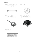
SECTION 2 INSTALLATIONS 2.1 System Installation 2.1.1 CPU Installation (IP-4MTS6B series) Carefully follow the steps below in order to install the CPU: 1. Check and confirm that you are going to install correctly CPU type and pin numbers (figure 3). 2. Take the screwdriver and releasing screw-nut of the socket 479. 3. Rotate mark of screw-nut to face the “OPEN”. 4. Align the pins of the CPU against the pinholes of the socket 479. Be sure to pay attention to the orientation of the CPU.
Installations Removing a CPU: 1. Before removing the CPU, turn off the IP-4MTS6B series power; then wait for about 20 minutes until the heat radiation plate of the cooling fan and the CPU cools down. 2. Rotate mark of screw-nut to face the “OPEN”. 3. To remove the CPU. Note: The CPU and the heat radiation plate are hot. They may cause burns. To remove the CPU, reverse the installation steps. 2.1.2 Heat Sink Installation Make sure that good contact is made between the processors and the heat sinks & fan.
Installations 2.1.3 Memory Module Installation Figure 5 display the notch marks and what they should look like on your DIMM memory module. DIMMs have 184-pins and two notches, that will match with the onboard DIMM socket. DIMM modules are installed by placing the chip firmly into the socket at a 90-degree angle and pressing straight down (figure 6) until it fits tightly into the DIMM socket.
Installations Carefully follow the steps below in order to install the DIMMs: 1. To avoid generating static electricity and damaging the DIMM, ground yourself by touching a grounded metal surface or using a ground scrap before you touch the DIMM. 2. Do not touch the connector of the DIMM. Dirt residue may cause a malfunction. 3. Hold the DIMM with its notch to the front side of the IP-4MTS6B series and insert it completely into the socket. A DIMM should be inserted into the inner socket first.
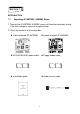
Installations 2.1.4 Setting Jumpers There are jumpers on the Embedded Board of the IP-4MTS6B series. You can set the jumpers to make the necessary operations. Figure 7: Jumper Connector For any three-pins jumpers (Figure 7), the jumper setting is 1-2 when the jumper connects pins 1 and 2. The setting is 2-3 when pins 2 and 3 are connected and so on. You see one of the lines surrounding a jumper, which indicates pin NO.1.
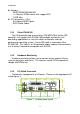
Installations 2.2 Board Layout IP-4MTS6B Jumper & Connector Location 93004 CN4 KB/MS IR-CONN VGA CN1 LAN1-LED LAN2-LED COM1 CN2 CN5 CN3 CN8 LPT1 JP1JP2 LAN2 LAN1 CN6 USB2/3 CN7 USB0/1 EXT.
Installations 2.3 Jumper Setting Table for Jumper Location Description: Use the information in the following table to change the jumpers.
Installations In order to set up the correct configuration, here is the description about how to set the jumpers to enable/disable or change functions. All jumpers’ location please refer to jumper location diagram.
Installations LCD power setting select: JP6 Function JP4 3.
Installations 2.4 Connector’s Description IP-4MTS6B Connector Location 93004 CN4 KB/MS IR-CONN VGA CN1 LAN1-LED LAN2-LED COM1 CN2 CN5 CN3 CN8 LPT1 JP1JP2 LAN2 LAN1 CN6 USB2/3 CN7 USB0/1 EXT.
Installations Table for Connector’s Location Description: Use the information in the following table to change the connector.
Installations CRT VGA port connector (D-SUB 15-pins female): CN1 Pin # Assignment Pin # Assignment 1 3 5 7 9 11 13 15 Red Blue Ground Ground VCC NC Hsync DDClk 2 4 6 8 10 12 14 Green NC Ground Ground Ground DDData VSync y Figure: 5 1 15 11 COM1 RS-232 serial port connector (D-Sub 9-pins male): CN2 Pin # Assignment Pin # Assignment 1 2 3 4 5 DCD (Data Carrier Detect) RXD (Receive Data) TXD (Transmit Data) DTR (Data Terminal Ready) Ground 6 7 8 9 DSR (Data Set Ready) RTS (Request to Send) CTS
Installations Parallel port connector (D-Sub 25-pins female): CN3 Pin # Assignment Pin # Assignment 1 2 3 4 5 6 7 8 9 10 11 12 13 Line Printer Strobe PD 0, Parallel Data 0 PD 1, Parallel Data 1 PD 2, Parallel Data 2 PD 3, Parallel Data 3 PD 4, Parallel Data 4 PD 5, Parallel Data 5 PD 6, Parallel Data 6 PD 7, Parallel Data 7 ACK, Acknowledge Busy Paper Empty Select 14 15 16 17 18 19 20 21 22 23 24 25 Auto Feed Error Initialize Select Ground Ground Ground Ground Ground Ground Ground Ground y Figure: 13
Installations PS/2 keyboard connector (6-pins purple mini Din): CN5 Pin # Assignment Pin # Assignment 1 3 5 Keyboard data Ground Keyboard clock 2 4 6 NC +5V NC y Figure: 6 5 4 3 2 1 PS/2 mouse connector (6-pins green mini Din): CN5 Pin # Assignment Pin # Assignment 1 3 5 Mouse data Ground Mouse clock 2 4 6 NC +5V NC y Figure: 6 5 4 3 2 22 1
Installations Gigabit Ethernet RJ-45 (LAN2) connector (RJ-45 phone-jack): CN6 Pin # Assignment Pin # Assignment 1 2 3 4 Transmit output (+) Transmit output (-) Receive input (+) NC 5 6 7 8 NC Receive input (-) NC NC y Figure: USB 2/3 connectors (4-pins female): CN6 Pin # Assignment Pin # 1a 2a 3a 4a VCC USB2 USB2 + Signal ground Assignment 1b 2b 3b 4b VCC USB3 USB3 + Signal ground y Figure: 23 1 4 1 4
Installations Gigabit Ethernet RJ-45 (LAN1) connector (RJ-45 phone-jack): CN7 Pin # Assignment Pin # Assignment 1 2 3 4 Transmit output (+) Transmit output (-) Receive input (+) NC 5 6 7 8 NC Receive input (-) NC NC y Figure: USB 0/1 connectors (4-pins female): CN7 Pin # Assignment Pin # 1a 2a 3a 4a VCC USB0 USB0 + Signal ground Assignment 1b 2b 3b 4b VCC USB1 USB1 + Signal ground y Figure: 24 1 4 1 4
Installations External keyboard & mouse connector (6-pins pin-header): CN8 Pin # Assignment Pin # Assignment MS Clock MS Data 1 2 KB Clock KB Data 3 4 Ground VCC 5 6 y Figure: 1 6 COM2 RS-232 serial port connector (10-pins pin-header): CN9 Pin # Assignment Pin # Assignment 1 2 3 4 5 DCD RXD TXD DTR Ground 2 4 6 8 10 DSR RTS CTS RI 5V y Figure: 25 9 1 10 2
Installations 18/24Bits LVDS panel interface (40-pins male): CN10 Pin # Assignment Pin # Assignment 1 3 5 7 9 11 13 15 17 19 21 23 25 27 29 31 33 35 37 39 NC Ground YAM0 YAP0 Ground YAM2 YAP2 Ground YAM3 YAP3 Ground YBM1 YBP1 Ground CLKBM CLKBP NC NC NC LCD_BKL 2 4 6 8 10 12 14 16 18 20 22 24 26 28 30 32 34 36 38 40 NC Ground YAM1 YAP1 Ground CLKAM CLKAP Ground YBM0 YBP0 Ground YBM2 YBP2 Ground YBM3 YBP3 +12V +12V VCC_LCD VCC_LCD y Figure: 40 2 39 1 26
Installations USB 4/5 connector (9-pins pin-header): CN11 Pin # Assignment Pin # 1 3 5 7 9 VCC USB4 USB4 + Ground --- Assignment 2 4 6 8 10 VCC USB5 USB5 + Ground NC y Figure: System fan power connector: CN13 Pin # 1 2 3 2 10 1 9 Assignment Ground VCC Fan Status Signal y Figure: 3 27 1
Installations CPU fan power connector: CN14 Pin # 1 2 3 Assignment Ground VCC Fan Status Signal y Figure: 3 Audio Line_out pin-header: CN15 Pin # 1 Assignment 1 2 3 4 LOUT_L Ground Ground LOUT_R y Figure: 1 28 4
Installations Secondary IDE connector (40-pins 2.
Installations Floppy disk connector (34-pins 2.
Installations CD_IN pin-header: CN18 Pin # Assignment 1 2 3 4 CD_IN_Left CD_GND CD_GND CD_IN_Right y Figure: 1 20-pins ATX power connector: CN19 Pin # Assignment Pin # 1 2 3 4 5 6 7 8 9 10 +3.3V +3.3V Ground +5V Ground +5V Ground NC 5VSB +12V 11 12 13 14 15 16 17 18 19 20 4 Assignment +3.
Installations Primary IDE connector (40-pins 2.
Installations System panel indicate connector: CN21 Pin # Assignment Pin # SPEAKER 1 3 5 7 +5V NC BZ SPKR 2 4 6 5V NC Ground KEYLOCK HDD LED 9 11 Assignment PWR LED 8 10 12 5V HDLED- KBLOCK Ground NC RESET 13 15 PWR ON RESET+ Ground 14 16 5VSB PWRBT- y Figure: LAN2 LED pin-header: JP1 Pin # Assignment 1 3 LINK_LED ACT_LED 2 16 1 15 Pin # Assignment 2 4 VCC_3V VCC_3V y Figure: 2 4 1 3 33
Installations LAN1 LED pin-header: JP2 Pin # Assignment 1 3 LINK_LED ACT_LED Pin # Assignment 2 4 VCC_3V VCC_3V y Figure: 2 4 1 3 34
SECTION 3 AWARD BIOS SETUP 3.1 BIOS Instructions Award’s ROM BIOS provides a built-in Setup program, which allows user to modify the basic system configuration and hardware parameters. The modified data will be stored in a battery-backed CMOS, so that data will be retained even when the power is turned off. In general, the information saved in the CMOS RAM will stay unchanged unless there is a configuration change in the system, such as hard drive replacement or a device is added.
Award BIOS Setup 3.2 Main Menu Once you enter the AwardBIOS™ CMOS Setup Utility, the Main Menu will appear on the screen. The Main Menu allows you to select from several setup functions and two exit choices. Use the arrow keys to select among the items and press to accept and enter the sub-menu.
Award BIOS Setup Power Management Setup: Use this menu to specify your settings for power management. See 3.8 for the details. PnP / PCI Configuration: This entry appears if your system supports PnP / PCI. See 3.9 for the details. PC Health Status: Use this menu to show your system temperature, speed and voltage status. See 3.10 for the details. Frequency / Voltage Control: Use this menu to specify your settings for frequency/voltage control. See 3.11 for the details.
Award BIOS Setup 3.3 Standard CMOS Features The items in Standard CMOS Setup Menu are divided into 10 categories. Each category includes no, one or more than one setup items. Use the arrow keys to highlight the item and then use the or keys to select the value you want in each item.
Award BIOS Setup IDE Secondary Master: Options are in its sub menu (described in 3.4) Press to enter the sub menu of detailed options. IDE Secondary Master: Options are in its sub menu (described in 3.4) Press to enter the sub menu of detailed options. Drive A/ Drive B: Options None 360K, 5.25 in/1.2M, 5.25 in/720K, 3.5 in/ 1.44M, 3.5 in/2.88M, 3.5 in Select the type of floppy disk drive installed in your system. Video: Options EGA/VGA/CGA 40/CGA 80/MONO Select the default video device.
Award BIOS Setup 3.4 IDE Adapters The IDE adapters control the hard disk drive. Use a separate sub menu to configure each hard disk drive. Phoenix - AwardBIOS CMOS Setup Utility IDE Primary Master IDE HDD Auto-Detection Press Enter IDE Primary Master Access Mode Auto Auto Capacity 13579 MB Cylinder Head Precomp Landing Zone Sector 26310 16 0 26309 63 Item Help ____________________________ Menu Level ¾¾ To auto-detect the HDD’s size, head...
Award BIOS Setup The following options are selectable only if the ‘IDE Primary Master’ item is set to ‘Manual’ Cylinder: Options Min = 0, Max = 65535 Set the number of cylinders for this hard disk.
Award BIOS Setup 3.5 Advanced BIOS Features This section allows you to configure your system for basic operation. You have the opportunity to select the system’s default speed, boot-up sequence, keyboard operation, shadowing and security.
Award BIOS Setup Thermal Management: It allows you to select the thermal Monitor. The Choice: Thermal monitor1, thermal Monitor2. Virus Warning: Allow you to choose the virus-warning feature for IDE Hard Disk boot sector protection. If this function is enabled and someone attempts to write data into this area, BIOS will show a warning message on screen and alarm beep.
Award BIOS Setup Swap Floppy Drive: If the system has two floppy drives, you can swap the logical drive name assignments. The choice: Enabled, Disabled. Boot Up Floppy Seek: Seeks disk drives during boot up. Disabling speeds boot up. The choice: Enabled, Disabled. Boot Up NumLock Status: Select power on state for NumLock. The choice: On, Off. Gate A20 Option: Select if chipset or keyboard controller should control GateA20. Normal---A pin in the keyboard controller controls GateA20.
Award BIOS Setup Note: To disable security, select PASSWORD SETTING at Main Menu and then you will be asked to enter password. Do not type anything and just press , it will disable security. Once the security is disabled, the system will boot and you can enter Setup freely. APIC Mode: This item allows you to enable APIC (Advanced Programmable Interrupt Controller) functionality. APIC is an Intel chip that provides symmetric multiprocessing (SMP) for its Pentium systems.
Award BIOS Setup 3.6 Advanced Chipset Features This section allows you to configure the system based on the specific features of the installed chipset. This chipset manages bus speeds and access to system memory resources, such as DRAM and the external cache. It also coordinates communications between the conventional ISA bus and the PCI bus. It must be stated that these items should never need to be altered.
Award BIOS Setup Active To Precharge Delay: Select the operating system that is active to precharge delay. The choice: 5, 6, 7. DRAM RAS# To CAS# Delay: This field let’s you insert a timing delay between the CAS and RAS strobe signals, used when DRAM is written to, read from, or refreshed. Fast gives faster performance; and Slow gives more stable performance. This field applies only when synchronous DRAM is installed in the system. The choice: 2, 3.
Award BIOS Setup Memory Hole At 15M-16M: You can reserve this area of system memory for ISA adapter ROM. When this area is reserved, it cannot be cached. The user information of peripherals that need to use this area of system memory usually discusses their memory requirements. The choice: Enabled, Disabled. Delayed Transaction: The chipset has an embedded 32-bit posted write buffer to support delay transactions cycles. Select “Enabled” to support compliance with PCI specification version 2.2.
Award BIOS Setup 3.
Award BIOS Setup IDE Primary/Secondary Master/Slave PIO: The four IDE PIO (Programmed Input/Output) fields let you set a PIO mode (0-4) for each of the four IDE devices that the onboard IDE interface supports. Modes 0 through 4 provide successively increased performance. In Auto mode, the system automatically determines the best mode for each device. The choice: Auto, Mode 0, Mode 1, Mode 2, Mode 3 and Mode 4.
Award BIOS Setup USB Keyboard Support: Select “Enabled” if your system contains a Universal Serial Bus (USB) controller and you have a USB keyboard. The choice: Enabled, Disabled. USB Mouse Support: Select “Enabled” if your system contains a Universal Serial Bus (USB) controller and you have a USB mouse. The choice: Enabled, Disabled. AC97 Audio: This item allows you to decide to auto or disable the chipset family to support AC97 Audio. The choice: Auto, Disabled.
Award BIOS Setup Power On Function: Options Password, Hot KET, Any KEY, BUTTON and Keyboard 98. You can use this item to select operating Power On the system. KB Power ON Password: Option Enter You can set password to limit operating KB Power On system. Hot Key Power ON: Options Ctrl+F1 ~ Ctrl+F12 You can use this item to select operating Hot Key to Power On system.
Award BIOS Setup Use IR Pins: This item allows you to select IR transmission routes, one is RxD2, TxD2 (COM Port) and the other is IR-Rx2Tx2. The choice: IR-Rx2Tx2, RxD2 and TxD2. Onboard Parallel Port: This item allows you to determine access onboard parallel port controller with which I/O address. The choice: 3BC/IRQ7, 378/IRQ7, 278/IRQ5 and Disabled. Parallel Port Mode: Select an operating mode for the onboard parallel (printer) port.
Award BIOS Setup 3.8 Power Management Setup The Power Management Setup allows you to configure you system to most effectively save energy while operating in a manner consistent with your own style of computer use.
Award BIOS Setup Video Off In Suspend: This determines the manner in which the monitor is blanked. The choice: Yes, No. Suspend Type: This determines the CPU status during power saving mode. The choice: PwrOn Suspend, Stop Grant. Suspend Mode: When “Enabled” and after the set time of system inactivity. All devices except the CPU will be shut off. The choice: Disabled, 1, 2, 4, 8, 12, 20, 30, 40 Min and 1Hour.
Award BIOS Setup PM Events: PM events are I/O events whose occurrence can prevent the system from entering a power saving mode or can awaken the system from such a mode. In effect, the system remains alert for anything, which occurs to a device, which is configured as Enabled, even when the system is in a power down mode.
Award BIOS Setup 3.9 PnP/PCI Configurations This section describes configuring the PCI bus system. PCI, or Personal Computer Interconnect, is a system, which allows I/O devices to operate at speeds nearing the speed the CPU itself uses when communicating with its own special components. This section covers some very technical items and it is strongly recommended that only experienced users should make any changes to the default settings.
Award BIOS Setup Resource controlled by: The Award Plug and Play BIOS has the capacity to automatically configure all of the boot and Plug and Play compatible devices. However, this capability means absolutely nothing unless you are using a Plug and Play operating system such as Windows®95. If you set this field to “Manual” choose specific resources by going into each of the sub menu that follows this field (a sub menu is preceded by a “¾”). The choice: Auto (ESCD), Manual.
Award BIOS Setup 3.10 PC Health Status Phoenix - AwardBIOS CMOS Setup Utility PC Health Status CPU Warning Temperature SYS Temperature CPU Temperature CPU Fan Speed SYS Fan Speed VCC_2V5 VCORE 3.3V +5V +12 V -12V -5V VBAT (V) 5VSB (V) Shutdown Temperature Disabled 34°C/93°F 40°C/104°F 5010RPM 5213RPM 2.48V 1.29V 3.28V 4.97V 12.03V -11.54V -5.20V 3.02V 4.
Award BIOS Setup 3.11 Frequency/Voltage Control Phoenix - AwardBIOS CMOS Setup Utility Frequency/Voltage Control Auto Detect PCI CLK Spread Spectrum Enabled Disabled Item Help ____________________________ Menu Level ¾ ↑↓←→Move Enter: Select +/-/PU/PD: Value F10: Save ESC: Exit F1: General Help F5: Previous Values F6: Fail-safe defaults F7: Optimized Defaults Auto Detect PCI CLK: When “Enabled”, this item will auto detect if the PCI slot have devices and will send clock signal to PCI devices.
Award BIOS Setup 3.12 Load Fail-Safe Defaults When you press on this item you get a confirmation dialog box with a message similar to: Load Fail-Safe Defaults (Y/N)? N Pressing ‘Y’ loads the BIOS default values for the most stable, minimal-performance system operations. 3.
Award BIOS Setup 3.14 Supervisor/User Password Setting You can set either supervisor or user password, or both of then. The differences between are: Set Supervisor Password: can enter and change the options of the setup menus. Set User Password: just can only enter but do not have the right to change the options of the setup menus. When you select this function, the following message will appear at the center of the screen to assist you in creating a password.
Driver Utility Installation 3.15 Exit Selecting Save & Exit Setup Pressing on this item asks for confirmation: Save to CMOS and EXIT (Y/N)? Y Pressing “Y” stores the selections made in the menus in CMOS – a special section of memory that stays on after you turn your system off. The next time you boot your computer, the BIOS configures your system according to the Setup selections stored in CMOS. After saving the values the system is restarted again.