
user manual


Award BIOS Setup
46
3.6 Advanced Chipset Features
This section allows you to configure the system based on the specific
features of the installed chipset. This chipset manages bus speeds and
access to system memory resources, such as DRAM and the external
cache. It also coordinates communications between the conventional ISA
bus and the PCI bus. It must be stated that these items should never need
to be altered. The default settings have been chosen because they provide
the best operating conditions for your system. The only time you might
consider making any changes would be if you discovered that data was
being lost while using your system.
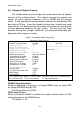
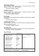
Phoenix - AwardBIOS CMOS Setup Utility
Advanced Chipset Features
DRAM Timing Selectable
X CAS Latency Time
X Active To Precharge Delay
X DRAM RAS# To CAS# Delay
X DRAM RAS# Precharge
DRAM Data Integrity Mode
MGM Core Frequency
System BIOS Cacheable
Video BIOS Cacheable
Memory Hole At 15M-16M
Delayed Transaction
Delay Prior To Thermal
AGP Aperture Size (MB)
** On-Chip VGA Setting **
On-Chip VGA
On-Chip Frame Buffer Size
Boot Display
Panel Scaling
By SPD
2.5
7
3
3
Non-ECC
Auto Max 266MHz
Enabled
Disabled
Disabled
Enabled
16Min.
64
Enabled
32MB
CRT
Auto
Item Help
____________________________
Menu Level ¾
↑↓←→Move Enter: Select +/-/PU/PD: Value F10: Save ESC: Exit F1: General Help
F5: Previous Values F6: Fail-safe defaults F7: Optimized Defaults
DRAM Timing Selectable:
Select the operating system that is selecting DRAM timing, so select SPD
for setting SDRAM timing by SPD.
The choice: Manual, By SPD.
CAS Latency Time:
When synchronous DRAM is installed, the number of clock cycles of CAS
latency depends on the DRAM timing.
The choice: 2, 2.5.