
Accelerated Graphics Port Interface Specification

AGP3.0 Interface Specification
Rev. 1.0
18
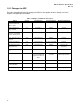
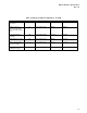
Table 6: AGP3.0 New Signals
Name Type of
Change
Type Description
AGP_Vrefcg
Redefined Static
This pin is used by the motherboard (or core-logic) to supply AGP Vref or
AGP3.0 Vref to the graphics card based on the configuration detected.
AGP_Vrefgc
Redefined Static This pin is used by the Graphics Card to supply AGP or AGP3.0 Vref to the
motherboard based on the configuration detected.
GC_DET#
New Static This is pulled down to Vss by the AGP3.0 or Universal AGP3.0 Graphics
Card. Other AGP Graphics Cards will leave this signal unconnected. The
motherboard usage of this pin is implementation specific
This signal uses a currently “reserved” pin on the AGP connector.
MB_DET#
New Static This is pulled down to Vss by the AGP3.0 or Universal AGP3.0
motherboard. The graphics card usage of this pin is implementation
specific.
This signal uses a currently “reserved” pin on the AGP connector.
DBI_HI
New Source Synchronous
This is a bit that goes along with AD[31:16] to indicate whether
AD[31:16] needs to be inverted on the receiving end.
DBI_HI = 0 AD[31:16] is not inverted, so receiver may use as is.
DBI_HI = 1 AD[31:16] is inverted, so receiver must invert before use.
On the AGP connector, DBI_HI is multiplexed with the signal, PIPE#,
which is not used in AGP3.0.
DBI_LO
New Source Synchronous
This is a bit that goes along with AD[15:00] to indicate whether
AD[15:00] needs to be inverted on the receiving end.
DBI_LO = 0 AD[15:00] is not inverted, so receiver may use as is.
DBI_LO = 1 AD[15:00] is inverted, so receiver must invert before
use.
This signal uses a currently “reserved” pin on the AGP connector.
2.1.2 Clocking Changes
Table 5 describes the signaling rate and the clocking scheme associated with the signals on the
AGP3.0 interface. The major change from AGP is that the source synchronous signals are “strobed” at
8X the common clock frequency of 66 MHz. All signals that are clocked using the common clock retain
the signaling rate of AGP. The names of the strobes used to clock the Source Synchronous signals
have been changed from those used in AGP, to more accurately specify their usage.
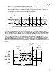
Figure 2-1 illustrates the effect of the 8X signaling on the Side-band Address (SBA) interface. T3, T2
and T1 stand for Type 3, 2 and 1 SBA requests, each of which is sent in two 8-bit parts labeled H and L.
Note that there is an additional request type not shown in this example called Type 4 used for memory
addresses beyond 36 bits. NOP reflects an idle bus where the SBA# signals are 1s or in low voltage
level state. Description of these request types may be found in the AGP Interface Specification. Some
points to be noted follow.
1. To initiate a new memory transaction, an AGP Master may need to generate anywhere from one
to all four request Types. A complete request bundle including Types 4, 3, 2, and 1 now fits into
one, common clock cycle in AGP8X. Such a request requires two common clock cycles in
AGP4X and four common clock cycles in AGP2X.
2. While it is possible to initiate multiple transactions
2
in one common clock cycle, AGP enforces a
rule of at most one transaction per common clock cycle. The first Type request of a transaction
2
A transaction is initiated by a Type 1 request, which triggers the core-logic to begin execution. Types 2 through 4 requests
do not initiate a transaction hence any number of these can be sent in a common clock cycle.