
Accelerated Graphics Port Interface Specification

AGP3.0 Interface Specification
Rev. 1.0
55
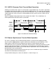
3.2.1 AGP3.0 Common Clock Transfer Mode Operation
All timings for common clock signals are referenced to a single 66 MHz clock. This clock is required to
be common between the two agents at each end of the AGP3.0 channel. This clock may or may not be
synchronous to some other clock in the system (e.g. the FSB clock). If there is more than one AGP3.0
segment within the system, it must be assumed that different base clocks have been used by each of
the segments.
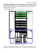
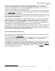
Figure 3-2 highlights timing relationships for the common clock mode. These relationships are
unchanged from that of the AGP interface specification.
Common
clock
Data1
Data2
Data1 Data2
Data at
transmitter
Data at
Receiver
T1 T2
t
VAL(MAX)
t
VAL(MIN)
t
H
t
SU
t
Flt
Figure 3-2: Common Clock Transfer Timings
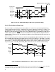
3.2.2 Source Synchronous Transfer Mode Operation
The source synchronous transfer mode operation provides a mechanism for multiplying the data
transfer rate of the AD[31:0] data bus signals relative to the common (base) clock frequency. In this
mode, 32 bytes of data are transferred during a time equal to a single common clock cycle.
As in AGP2.0, the source synchronous clock mode is implemented as a timing layer below the baseline
protocol’s flow control mechanisms. This timing layer, referred to below as the inner loop, specifies
timing relationships for the reliable transfer of data from the output latches at the transmitting device to
the input latches at the receiving device.
The logical protocol mechanisms operate above this layer, in the so-called outer loop, to control the
actual transfer of data between the data queues.
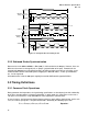
A simple model showing these various time domains is shown in Figure 3-3: