
Accelerated Graphics Port Interface Specification

AGP3.0 Interface Specification
Rev. 1.0
58
Receive
AD_STBS
Receive
Data
Data1 Data2
Receive
AD_STBF
t
RX_H
t
RX_SU
Data4 Data5 Data6 Data7
Data0
t
RX_SU
t
RX_H
Data3
Common Clk
(66 MHz)
t
RS8su
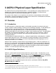
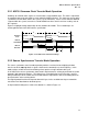
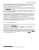
Figure 3-5: Receive Strobe/Data Timings for 8X Source Synchronous Timing
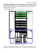
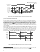
3.2.2.3 Receive Inner to Outer Loop:
The most complex set of timings are those that address the receiver inner to outer loop relationships.
To better understand these timings, a model of the inner to outer loop transfer interface is required. For
the following discussion, refer to the receiver transfer diagram shown Figure 3-6.
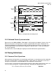
15
In the case of the
AD interface (after the fourth rising edge of the receiver AD_STBS strobe), eight DWords of valid data are
available to the target core. Data is then transferred from the inner loop to the outer loop based on the
common clock. In many respects, the challenge is to define a circuit to reliably affect this transfer for all
system conditions.
Figure 3-5 depicts the possible minimum and maximum AD_STBF/AD_STBS relationships at the receiver
in the 8X mode. When two consecutive data transfers occur, the first of these is described as occurring
in T1. In the minimum [AD_STBF/AD_STBS] strobe delay, all eight rising strobe edges are guaranteed to
occur during T1. For the maximum strobe delay, however, there can be a variable number (less than
four) of rising edges for the AD_STBF and AD_STBS strobes that cross the common clock boundary.
Common clk
Receive
AD_STBS
(min)
Receive
AD_STBS
(max)
T1
T2
8 Dwords Received
8Dwords Received
Strobe uncertainty
T
RS8su
T
RS8h
Figure 3-6: Minimum and Maximum Inner to Outer Loop Receive Timings
15
Note that the diagram shows only the AD_STBS waveform. References that appear to be to the falling edge of AD_STBS
are actually to the rising edge of AD_STBF. As previously noted, the strobes are not to be used differentially.