
Accelerated Graphics Port Interface Specification

AGP3.0 Interface Specification
Rev. 1.0
60
t
DVb
t
DVa
Common
Clock
Transmit
data
Transmit
ADSTBF
Data7Data6Data5Data4Data3Data2Data1Data0
t
TSf(min)
Transmit
data
Transmit
ADSTBF
Data5Data4Data2Data1
t
DVa
t
DVb
Data3
t
Dva
t
DVb
Common
Clock
Transmit
data
Transmit
ADSTBS
Data13Data12Data11Data10Data9Data8Data7Data6
t
TS8r(max)
Data0
T1
T2
t
TS8r(max)
t
TS8r(max)
extends into T2
Transmit
ADSTBS
Minimum
timings
Maximum
timings
T1 Phase
T2 Phase
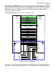
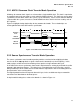
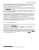
Figure 3-7: Composite Receive Timing for 8X
3.2.3 Sideband Strobe Synchronization
Data transfer on the Sideband Address Port (SBA) is similar to that for the AD port. However, there are
differences that must be managed (such as proper synchronization of the port). Protocol rules for
managing the SBA port are unchanged from those of AGP2.0; logical extension for such things as the
number of AGP3.0 NOP commands prior to stopping the sideband strobes, restart synchronization,
etc., is to be expected.
Also noted earlier is that the SBA port is logically inverted for AGP3.0 with regard to AGP2.0.
3.3 Timing Definitions
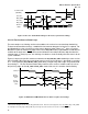
3.3.1 Common Clock Operations
During common clock operations, the signal timing specifications are based purely on their relationship
to the base clock operating at a frequency of 66 MHz. In other words, the signal at the receiver must
satisfy the receiver latches’ setup and hold times with regard to the common clock.
In most instances, the interconnect distance between two bus agents will be relatively long, and in such
cases, the critical speed path is setup time limited and is defined by the following expression:
T
CYC
> T
VAL(max)
+ T
FLT(max)
+ T
SU
+ T
SKEW
Equation 1