
Accelerated Graphics Port Interface Specification

AGP3.0 Interface Specification
Rev. 1.0
62
• ISI
17
due to imperfect impedance matching resulting from tolerances on package, board
trace, connector, driver and receiver impedances
• Rising/falling edge delay matching
• Vref uncertainty
• Core circuitry noise effects (i.e., clock jitter)
• Package pad-to-pin length variation
• Skew between the data and strobe signals on the motherboard and graphics card (due to
trace length mismatch and coupling effects, as well as RPD
18
at the connector)
• Skew between the data and strobe signals on the sending chip (including package SSO
19
and RPD effects)
• Skew between the data and strobe signals on the receiving chip (input capacitance
mismatches and timing path mismatches)
• Guard band and other allowances for testing
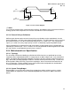
Source synchronous operation implies the placement of the strobe in “quadrature” with respect to the
data. Therefore, the sum of silicon and interconnect skews plus the time required to meet the setup or
hold times at the receiver latch must be less than ½ bit time. At 8X speeds this is 937.5 pS. For
AGP3.0, the quantitative effects of the interconnect have been evaluated for worst-case parametric
variations and are incorporated in the timing skew budget.
The skew of the data relative to the associated strobe is only visible as the specs T
DVb
and T
Dva
.
The following timing relationships must be met for source synchronous timing:
T
INTC_SUS
+ T
RX_SU
<= T
DVb
Equation 3
T
INTC_HS
+ T
RX_H
<= T
DVb
Equation 4
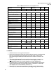
Definitions for the 8X timings are provided in Table 32. (AGP3.0 4X speeds are the same as for AGP2.0
4X mode – see table 42.) Note that the interconnect skew targets listed are “pad-to-pad,” covering the
AGP3.0 channel from the transmitter pad to the receiver pad.
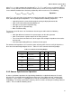
Table 32: Source Synchronous Skew Timing Budget
Symbol Setup Hold Description
Budget 937.5 937.5 Source synchronous setup/hold skew budget
T
DVb
527.5 Total setup data valid at the driver/transmitter pins in ps
T
DVa
477.5 Total hold data valid at the driver/transmitter pins in ps
T
RX_SU
85 Total setup at the receiver in ps
T
RX_H
210 Total hold at the receiver in ps
T
INTC_SUS
442.5 Total interconnect setup skew from pad to pad in ps
T
INTC_HS
267.5 Total interconnect hold skew from pad to pad in ps
17
Inter-Symbol Interference: This includes the effects of impedance mismatches and coupling on a sequence of edge
transitions.
18
Return Path Discontinuity
19
Simultaneous Switching Outputs