
Accelerated Graphics Port Interface Specification

AGP3.0 Interface Specification
Rev. 1.0
63
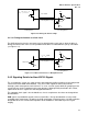
The AGP3.0 Design Guide provides an example distribution of first and second order timing budget
effects impacting signal skew.
The previous discussion is directed at inner loop timings. Timing specifications between the inner and
outer loops must also be closely managed. Specifically, the system must be designed to ensure that
data sent in conjunction with T1 is available for capture, in the common (base) clock domain, at the end
of T2. This imposes constraints on such design parameters as flight time, and buffer output delays, as
well as clock skew. All of the clock skew parameters of both common clock mode and source
synchronous mode must be analyzed and controlled to ensure safe data transfer between the clock
domains.
3.4 Interface Signaling
AGP3.0 specifies two basic signal types, generally referred to as AGP3.0 signals; these are the source
synchronous signals for data transfer and common clock signals for arbitration and control. There is a
third type of signal (termed “asynchronous”) that is bound to no particular (AGP3.0) clock domain
whatsoever and deals solely with out-of-band communications.
3.4.1 AGP3.0 Signaling Details
3.4.1.1 Signaling Levels
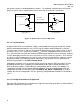
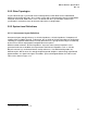
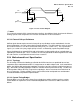
AGP3.0 specifies a 0.8 V voltage swing, end terminated, and referenced to V
SS
, as opposed to AGP2.0,
which specified a rail-to-rail 1.5 V series terminated voltage swing.
This change permits a higher data rate and a common signaling voltage, which can be realized for
multiple-generations of silicon technology. Figure 3-8 shows the relationship between the V
DDQ
and V
SS
rails and the corresponding output voltage swing.
V
SS
V
DD
Q
= 1.5
Vref
= 0.35
Vswing
= 0.80
Figure 3-8: AGP3.0 Voltage Swing
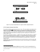
Simulations determined that the best termination value R
TT
is 50 Ω. If the driver pull-down also serves
as the termination, the N-channel device of the driver R
ON_N
should be set to this same value. The
series combination of the receiver’s termination R
TT
and the driver’s p-channel device R
ON_P
determines
the voltage swing for a positive transition V
OH
, the relationship that is shown in Figure 3-9. For a nominal
V
DDQ
of 1.5 volts and a target signal swing (V
SWING
) of 0.8 volts, this puts R
ON_P
at 43.75 Ω nominal.
The target V
SWING
level is 0.8 volts for a nominal V
DDQ
of 1.5 volts. The actual V
SWING
target is
proportionally dependent on the actual V
DDQ
. This level is obtained by the proper sizing of the driver