
Accelerated Graphics Port Interface Specification

AGP3.0 Interface Specification
Rev. 1.0
65
V
DDQ
V
OH
= 0.80V
Driving Device
R
TT
= Z
pd
Receiving Device
V
SS
R
ON_P
= Z
pd
(V
DD
/V
OH
- 1)
T-line impedance = Z
0
ref
V
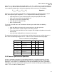
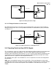
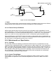
Figure 3-10: Driving the Interface High
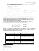
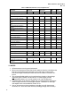
3.4.1.4 Driving the Interface to a Low Level
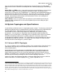
The AGP3.0 interface has the same make-up in its default (or quiescent) state as when the driver is
driving the interface low. In this case the pull-down of the driver is enabled while its pull-up is disabled
(see Figure 3-11).
R
ON_N
= Z
pd
V
OL
= V
SS
= 0.00V
Driving Device
R
TT
= Z
pd
Receiving Device
V
SS
V
SS
T-line impedance = Z
0
ref
V
Figure 3-11: A Quiescent Interface or Being Driven Low
3.4.2 Signaling Details for Non-AGP3.0 Signals
The “asynchronous” signals are signals that are not bound to the AGP3.0 clocking scheme and provide
some level of out-of-band communication. They are used to support the Universal Serial Bus,
interrupts, power management, and such basics as reset. Several signals within this grouping present
special concerns for the component and system designer. Although briefly described in this section,
requirements for these signals have not changed from AGP2.0.
The (common) clock signal is also included here, since its requirements also have not changed from
that of AGP2.0.
USB signals are provided to support a Universal Serial Bus. Design considerations must be made
according to the requirements set forth by the USB specification. Interposing traces for USB need to be
designed to 45 Ω ±15% to match the impedance of the USB drivers and cable to preserve signal
integrity.