
Accelerated Graphics Port Interface Specification

AGP3.0 Interface Specification
Rev. 1.0
68
S
H
trace
trace
Ground reference plane
H’
reference plane 1
Stripline Interconnect
S
H
trace
trace
Ground reference plane
Microstrip Interconnect
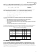
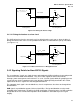
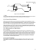
Figure 3-12: Spacing to Height Definitions for Stripline and Microstrip Implementations
3.5.3.2 System (Common) Clock Skew
The maximum allowable, total common clock skew is 1.0 ns. This value includes skew and jitter, which
originates on the motherboard and clock synthesizer, and represents the amount of skew observed
between the clock inputs to the transmitter’s output latches and those of the AGP3.0 Master and target
receiver’s input latches. Clock skew must be evaluated not only at a single threshold voltage, but at all
points on the clock edge that fall within the switching range of the rising edge of the common clock as
shown in Figure 3-13
22
.
The total skew is allocated such that 0.1 ns originates from the add-in card routing, and 0.9 ns originates
from the motherboard routing and clock synthesizer. The motherboard designer shall determine how
the 0.9 ns value is allocated between the board and the synthesizer. To correctly evaluate clock skew,
the system designer must take into account clock distribution on the add-in board as specified in the
following section.
Common clock skew is measured between the pins of the two AGP3.0 devices at the rising clock edge
only; duty cycle is independent of the AGP3.0 interface design, and no specification exists regarding the
falling edge of clock.
22
The system designer may need to address an additional source of clock skew. This clock skew component occurs
between two devices that have clock input trip points at opposite ends of the V
il
- V
ih
range. In certain circumstances, this
can add to the clock skew measurement as described. Nevertheless, in all cases, actual total clock skew must be limited
to the specified number.