
Accelerated Graphics Port Interface Specification

AGP3.0 Interface Specification
Rev. 1.0
77
3.6 Component Level Electrical Specifications
This section provides details of the electrical characteristics for the AGP3.0 interface. I/O buffer design
technology to meet these requirements will not be addressed as it is beyond the scope of this
specification.
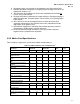
3.6.1 DC Specs
The parameters below list the DC requirements for the common clock and source synchronous modes
of AGP3.0.
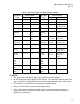
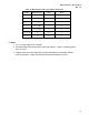
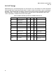
Table 38: DC Specifications for AGP3.0 Source Synchronous Signaling
Symbol Parameter Condition Min Max Units Notes
V
DDQ
I/O Supply Voltage 1.425 1.575 V
V
REF
Input reference voltage measured at
receiver pad
0.2333*Vddq-0.01
0.2333*Vddq+0.01
V 1
I
REF
Vref pin input current 0 < V
in
< V
DDQ
±50 µA 1
V
IH
Input High Voltage V
REF
+ 0.1 V
DDQ
V 1
V
IL
Input Low Voltage -0.3 V
REF
- 0.1 V 1
V
OH
Output High Voltage Standard 50Ω load
to ground.
0.5333*Vddq-0.05
0.5333*Vddq+0.05
V 2
V
OL
Output Low Voltage
I
out
= 1500 µA
0.05 V
C
DIE
Input Die Pad Capacitance
1.0 2.5 pF 3
Z
TERM
Terminator Equivalent
Impedance
V
OH
= 0.8V
Z
TARG
= 50 Ω
45 55 Ω 4
Z
PU
Pull-up Equivalent
Impedance
V
OH
= 0.8V
Z
TARG
= 50 Ω
39.3 48.2 Ω 5
/ NOTE
1. AGP3.0 requires differential input receivers to achieve the tight timing tolerances needed for
533MT/s. The nominal value of V
REF
is 0.350 V at V
DDQ
= 1.5 V and tracks V
DDQ
proportionally.
The given range can be designed using 1% resistors. The value of V
REF
is specified to be the
center point of the V
IL
/V
IH
range.
2. V
oh
is expected to be within 50 mV of V
SWING
at V
DDQ
=1.5 V and will track V
DDQ
proportionally.
Nominal (targeted) V
oh
= V
SWING
=0.8 V
3. Signal quality is significantly impacted by large die capacitance at the receiver pad.
Furthermore, to meet signal integrity requirements for 533 MT/s signaling, AGP3.0 devices are
required to be in high performance packages – modeled with appropriately detailed distributed
elements – with low overall inductance and capacitance (i.e., flip-chip BGA with 4 or more routing
layers).
4. The receiver terminator can also be used as the driver pull-down. To improve signal quality and
timing margin, the pull-down/terminator impedance should be as close as possible to its