
Accelerated Graphics Port Interface Specification

AGP3.0 Interface Specification
Rev. 1.0
88
3.6.6 Driver and Receiver Characteristics
3.6.6.1 AGP3.0 Driver Characteristics
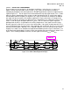
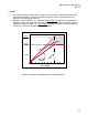
AGP3.0 is designed for point-to-point communication. The output driver must be able to deliver a
voltage swing of 0.8 V (nominal) to the terminated receiver (through the interconnect), with known
characteristic impedance Z
0
. To reduce signal skew, output buffers are designed to fit in the range
specified by the following V/I curves and have characteristics which are shown in Table 44 and Figure
3-22.
The minimum and maximum drive characteristics of the AGP3.0 output buffers are defined by V/I
curves. As with AGP2.0, these curves are interpreted as traditional “DC” transistor curves, except that
the curves are more linear than standard CMOS curves with a less pronounced saturation region
“knee.”
The terminator/pull-down device must be sufficiently linear to suppress reflections that can cause timing
skew. This linear region has to extend across the entire range between ground and 0.9 volts. The
linearity in the region beyond this point is not as critical, and the V-I curves are relaxed in this region.
The shape of the pull-up V-I characteristic also is not as critical. The driver pull-up must ensure,
however, that the signal swing is as close to the target Vswing of 0.8 volts (nominal) as possible into its
load. Making the pull-up more linear does cause the driver to present consistently stable impedance to
reflections on the bus, which decreases system noise and increases timing margin.
It is recommended that impedance compensated buffers with slew rate control mechanisms be used in
the I/O buffer design to maintain acceptable signal quality. The technological details required, describing
the implementation of output compensation or slew rate controls, are beyond the scope of this
specification. More information on compensated buffers can be found in the AGP3.0 Design Guide. In
addition to controlled impedance and slew, the data output buffers may need to be designed with
significant “rise and fall” delay matching across process, temperature, and voltage conditions.
Adherence to the V/I curves must be evaluated at worst-case system conditions, including the
tolerances on any components used to target the buffer impedance compensation. The minimum
curves must also be evaluated at minimum V
DDQ
and high temperature at the weakest process corner.
The maximum curve test points then should be evaluated at maximum V
DDQ
and low temperature at the
strongest process corner.
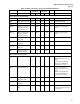
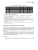
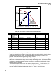
Table 44: Equations for Current Limits on Pull-down Driver and Terminator
Equation Description Condition Formula
1
Notes
A Max Limit 0 ≤ V
out
≤ V
DDQ
I
out
<
V
out
/ (0.9
*
Z
targ
)
B Min Limit V
OL(max)
< V
out
≤ V
swing
I
out
>
V
out
/ (1.1
*
Z
targ
)
C Min Limit
V
swing
< V
out
< 1.1*V
swing
I
out
>
V
swing
/ (1.1
*
Z
targ
) +
(V
out
– V
swing
) / (1.11
*
Z
targ
)
1
D Min Limit 1.1* V
swing
< V
out
≤ V
DDQ
I
out
>
V
swing
/ (1.1
*
Z
targ
) +
(0.1)
*
V
swing
/ (1.11
*
Z
targ
)
1
E Min Limit 0 < V
out
≤ V
OL(max)
I
out
≥ 0
Impedance Variation 0 < V
out
≤ V
swing
10%
2