
Accelerated Graphics Port Interface Specification
AGP3.0 Interface Specification
Rev. 1.0
92
3.6.6.5 Calibration of Driver Pull-up and Pull-down and Receiver Load
To maintain proper receiver load impedance and the proper signal swing (V
OH
), the driver and receiver
will need to be occasionally adjusted to account for changes in operating point. To support this activity, a
calibration mechanism has been developed for the AGP3.0 interface. The framework to support this
calibration mechanism (boot time requirements, calibration cycles, etc.) is described in section 2.1.4.
3.6.6.6 Component Die Considerations
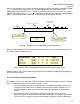
3.6.6.6.1 PHYSICAL LAYOUT RECOMMENDATIONS
Due to the high-speed signal transmission and fast turn-around time required for the AGP3.0 interface, it
is essential that custom layouts be employed throughout the portions of the component encompassing
the inner and outer (communication) loops and appropriately managed to optimize routing distances and
cell placements. In effect, all logic and circuit elements comprising the AGP3.0 interface may need to
be laid out as a single embedded block that bonds directly to the package lead tips.
3.6.6.6.2 DIE PAD DISTRIBUTION
In principle, the AGP3.0 channel is designed for AGP3.0 signals to be referenced to
ground throughout
the entire channel. Therefore, to achieve the necessary signal return paths, every buffer/driver should
have adequate bypass capacitance from V
DDQ
to Vss as close to the signal pad as possible. This
bypass capacitance should meet or exceed 100pF per high-speed output buffer to limit voltage collapse
resulting from simultaneous switching outputs.
Furthermore, there must be an adequate number of Vss pads distributed amongst the data and strobe
pads. The ratio for the number of die pads is listed in the following section (on packages) since there is
a strong relationship between the package type, this ratio, and the resulting signal characteristics. An
inadequate distribution of Vss pads can result in detrimental levels of ground bounce and SSO push out.
In addition to providing the necessary levels of bypass capacitance and proper number and placement
of Vss pads, the design should be such that strobe signals are placed in the center of their 16-bit data
group. This will help to reduce skew due to distribution variance of the input strobe signals along the
data buffers.
3.7 Package Considerations
There are two basic package types that have been evaluated and are provided here as a guide. These
package types are the flip-chip OLGA or FC-BGA and wirebond BGA packages. This section addresses
some of the issues and expectations associated with these packages and with package design
concerns in general.
Wirebond packages are not recommended for AGP3.0 signaling because of the large bond wire
inductance and crosstalk. Bond wires are usually closely spaced and have no signal return reference
plane nearby. The bond wires couple to their neighbors very efficiently causing crosstalk and timing
skew. The crosstalk can be reduced only at the expense of adding shielding ground wires around all
source synchronous signals.