
Accelerated Graphics Port Interface Specification
AGP3.0 Interface Specification
Rev. 1.0
93
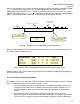
Simulations have shown that a wirebond suffers from potential power delivery resonance effects. The
cause for this is the LC circuit formed by the V
DDQ
/V
SS
bond wires and the on-die capacitance of the
driver. A certain amount of on-die capacitance is necessary since it decreases signal timing push-out
caused by simultaneous switching outputs (SSO). However, the C
ON_DIE
must be selected such that it
does not cause a resonance peak at a frequency where the data signals have significant spectral
energy.
Power delivery resonance must be carefully managed regardless of which package type is used. It is
sometimes helpful to insert a small resistance in series with the on-die decoupling capacitance to lower
the “Q” of the resonant circuit. The resistor value is a balance between sufficiently lowering the
resonance and maintaining the bypassing quality of the capacitance.
For both (all) package types it is important to:
• limit reflections due to impedance mismatches
• limit loop inductance and signal return path concerns
• limit trace-to-trace coupling
Package trace characteristic impedance should be matched to that of the terminator target value and
board interconnect to as great a degree as possible. Furthermore, package trace lengths should be
made as short as is reasonable. Matching trace lengths in the package removes the requirement for
compensating for package length mismatch on the board. However, be careful not to increase the inter-
signal coupling or loop inductance if matching is attempted. Note that these characteristics directly
impact T
Dvb
and T
Dva
.
Package traces may be microstrip, embedded stripline, or symmetric stripline as long as the package
impedance range is not exceeded. As with board routing, the strobes and corresponding signals within a
signal group are to be routed on the same layer(s), and are to be Vss referenced (this is true for the
entire channel and not just throughout the package).
The package designer is strongly encouraged to avoid routing signals such that they cross planes or
travel over voids for long distances. Bypass capacitance should be provided where possible to account
for coupling to signals and planes other than Vss.
Note that regardless of package type, signal current return path continuity must be carefully validated
through simulation for the complete channel: package, sockets, motherboard, cards, and connectors.
Such simulations should use models that are multi-line and fully coupled since pad-to-pad timings
(outlined in section 3.3.2) can be severely impacted by poor design choices with regard to the above
items.
3.7.1 Bump-out/Leadframe Requirements
As previously mentioned, the AGP3.0 channel is designed so that AGP3.0 signals are fully and
completely referenced to Vss throughout the entire channel. Therefore, to provide the necessary signal
return paths, an adequate number of Vss pads must be distributed amongst the data and strobe pads. It
is recommended that at least one die ground be supplied for every two AGP3.0 signals. Wirebond will
likely require a bond wire per AGP signal for the AC return path and additional wires for proper, low
inductance power delivery.
Example bondouts and pinouts are given in the AGP3.0 Design Guide.