
Accelerated Graphics Port Interface Specification
AGP3.0 Interface Specification
Rev. 1.0
94
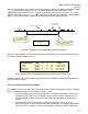
3.7.2 Pin-out/Ball-out Requirements
All AGP3.0 signal pins must be located to facilitate meeting the card connector with a minimum of
package/board vias or trace crossovers to minimize overall trace lengths, crosstalk, mismatched
number of layer changes, and trace length mismatches within a given signal group.
In addition, Strobe(s) and Vref signals must be properly grouped within their associated data groups:
AD_STBF[0], AD_STBS[0] with AD[15::00], C#/BE[1::0]
AD_STBF[1], AD_STBS[1] with AD[31::16], C#/BE[3::2] and DBI_HI and DBI_LO
SB_STBF and SB_STBS with SBA#[7::0]
To maintain a strong signal return path along Vss throughout the entire channel it is necessary to
provide adequate numbers of Vss pins distributed amongst the data and strobe pins. The ratio (or
better) for the number of AGP3.0 signals to Vss balls is recommended.
Ideally, VDDQ pins will be moved away from the region where signals and Vss traces and pins reside. If
not, then bypass capacitance should be added very near the package pins between the VDDQ and Vss
pins.
3.8 Power Delivery and Distribution
3.8.1 Power Supply Delivery
For AGP, the power supplied to the add-in card for its core supply (V
CC
) and I/O supply voltage (V
DDQ
)
must be separated on the die, package, and add-in card. Specifically, the I/O buffers must be powered
using V
DDQ
. For AGP3.0, the I/O buffers can be powered by a supply other than V
DDQ.
However,
component designers must be certain to manage noise coupling (such as) between the core and I/O
ring and to prevent excessive power supply droop.
As with AGP, the VCC3.3 and V
DDQ
power supplies must be sequenced such that the V
DDQ
voltage level
is never more than 0.5 V above the level of VCC3.3. Furthermore, V
DDQ
(supplied to the add-in card
through the connector) can never exceed 1.5 V.
The motherboard must connect all power supply pins on the connector as shown in the AGP Interface
Specification to guarantee proper current delivery and to provide proper AC signal return paths.
Likewise, the add-in card should also attach all connector power pins to appropriate power planes on
the card for good power delivery and signal returns. In addition, connector power pins should be
terminated to the Vss plane with high frequency, low inductance, decoupling capacitors.
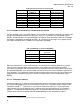
Add-in cards must use all ground pins, and any power pins not used must be bypassed to ground on the
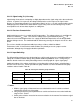
card with a good quality, low inductance 0.01 µF or larger capacitor. Table 47 lists the voltage ranges
for the supplies to the add-in card and the maximum currents that can be supplied via the connector.