
microATX Motherboard Interface Specification
microATX Motherboard Interface Specification
Version 1.2
Page 13
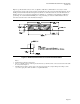
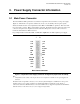
2.3.2 Disk I/O
The exact locations of the floppy, IDE, and/or SCSI I/O connectors are not specified. It is recommended that
they be placed along the front edge of the board (oriented as in Figure 3) to the right of the expansion slots.
When placing connectors, the designer should keep in mind that proper clearance must be provided for the
chassis peripheral bays.
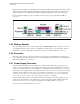
2.3.3 Front Panel I/O
The exact location of the front panel I/O connector is not specified. It is recommended that the connector be
placed along the front edge of the board (oriented as in Figure 3) to the right of the expansion slots. When
placing the connector, the designer should keep in mind that proper clearance must be provided for the chassis
peripheral bays. Locating the front panel I/O connector along the left edge of the board is not recommended
because of limited clearance with a full length add-in card.
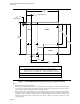
2.3.4 Back Panel I/O
With the PC platform evolving so fast, it makes sense to retain the greatest level of flexibility possible for the
future for external I/O. The multimedia explosion has demonstrated how user needs for enhanced I/O can
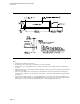
change quickly. Toward the rear of the chassis, the microATX and ATX Specifications define a stacked I/O
area that is 6.25 inches (158.75mm) wide by 1.75 inches (44.45mm) tall. This area allows the use of stacked
connectors on the motherboard to maximize the amount of I/O space available.
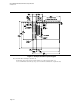
As shown in Figure 4, the bottom of the back panel opening is located 0.150 inches (3.81mm) below the top
of a typical 0.062 inch (1.57 mm) thick motherboard. A 0.1 inch (2.54 mm) required keepout zone is defined
around the perimeter of the cutout area, on both the inside and outside surfaces of the chassis back panel.
This keepout zone provides a reserved space that can be used to clip a chassis-independent I/O shield to the
chassis back panel. No slots, tabs, notches, or other topographical features should be placed within the
keepout zone. If a feature violates the keepout zone, the chassis loses the opportunity to support an I/O shield
that can be designed to fit all ATX chassis that meet the specifications listed below and detailed in Figure 4
and Figure 5. For best EMI attenuation performance, paint should not be applied within the keepout area,
because paint can prevent proper grounding of the I/O shield. Also, motherboard connector placement must
be limited as shown in Figure 5 to allow enough clearance between the connectors and chassis opening for the
I/O shield structure.