
microATX Motherboard Interface Specification

microATX Motherboard Interface Specification
Version 1.2
Page 17
2.4 Height Constraints
2.4.1 Primary (Component) Side Height Constraints
One of the major advantages of the microATX form factor is its backward-compatibility with the ATX
specification. The microATX motherboard can be installed in any ATX chassis with the addition of
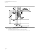
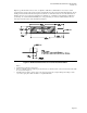
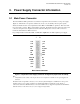
motherboard mounts. Table 6 lists the status of height constraints for specific areas. Figure 7 shows the
required maximum component height constraints for the components on the PC board. For full compliance
with microATX and to prevent interference with the chassis structure, power supply, or peripherals, the
motherboard components should not exceed the height limit in each zone defined. Similarly, microATX-
compliant power supplies, peripherals, and chassis features should not extend into the motherboard
component area.
Table 6: Height Constraints
Feature Status Comment
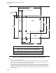
microATX motherboard maximum component heights Required See Figure 7.
microATX chassis keepout in Area A Required 3.0 inches (76.20mm) required; 3.5 inches
(88.90mm) is preferred.
The required chassis keepout for Area A is 3.0 inches (76.20mm) to facilitate dynamic considerations of
components in this area on the motherboard. The preferred (recommended) clearance is 3.5 (88.90mm)
inches to facilitate cooling solutions that require ducting. The bottom right corner of the board (as oriented in
Figure 7) is the most constrained because of the presence of 5.25-inch and 3.5-inch peripherals in some
chassis configurations. To maintain strict compliance to the microATX specification, careful placement of
peripherals, power supply, and chassis features is required.
2.4.2 Secondary (Bottom/Solder) Side Height Constraints
Required secondary (bottom) side motherboard height constraints for all areas (A-C, as shown in Figure 7) are
defined as follows (measured from the bottom planar surface of the motherboard PCB):
• ≤0.010” – Mounting hole standoff areas – no components. Restriction applies within 0.400” square area
centered on each required mounting hole location defined in Section 2.2. Nominal allowance is provided
only to accommodate slight reflow solder excess.
• ≤0.098” – All board circuit components (including leads) that are electrically conductive and intolerant of
direct connection to chassis ground (e.g., through-hole leads, surface mount resistors)
• ≤0.120” – Board components that are non-conductive or otherwise tolerant of direct connection to chassis
ground (e.g., connector guide/stake pins)
• ≤0.200” – Devices attached to the motherboard for the sole purpose of structural retention or stiffening
A chassis and its related elements (e.g., stiffening ribs, base pan, structural supports fasteners, etc.) must allow
≥0.250” clearance to the bottom planar surface of the motherboard PCB. This does not including mounting
hole standoffs, which may extend to and contact the PCB at the mounting holes within the prescribed 0.400”-
square areas.