
Accelerated Graphics Port Interface Specification

AGP3.0 Interface Specification
Rev. 1.0
16
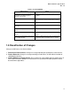
2 Description of New Features
This chapter describes the AGP3.0 features that differ from AGP2.0 and covers the following areas:
1. Signal Interface Differences
2. Transaction and Protocol Differences
3. Platform Dependencies
4. Programming Changes
The electrical specification that describes the signaling scheme is in Chapter 3. All other changes that
apply to the core specification are included in this chapter. Changes specific to Workstation platforms
are covered in Appendices A and B.
2.1 Signal Interface Differences
AGP3.0 uses the same signal list (with some additions) and connector level pin assignment as AGP2.0.
However, the signaling scheme is different. The new signaling scheme inverts the assertion levels of
many signals. For details on the signal functions, refer to AGP Interface Specification. The primary
motivation for doing this is to ensure that the unasserted logic state for any AGP3.0 signal is at “low
voltage” which equates to no DC current flow hence a low power state. Throughout this document, the
convention used for signal assertion is as follows:
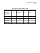
• A signal name which ends with # has logic ‘1’ = low voltage level (0V for AGP3.0) and logic ‘0’ =
high voltage (0.8V for AGP3.0).
• A signal name that does not end with # has logic ‘1’ = high voltage (0.8V on AGP3.0) and logic
‘0’ = low voltage (0V on AGP3.0).