
Accelerated Graphics Port Interface Specification

AGP3.0 Interface Specification
Rev. 1.0
27
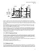
mode is enabled. The Master can initiate FRAME based cycles as soon as its BME bit is set in its
command register.
The reset condition sets the default value of PCAL_CYCLE to ‘0’, which translates to a 4ms period.
Once the initial calibration period is over, the normal operation is started by the core-logic. Calibration
Cycles can only start after the initial calibration period is completed. Calibration will precede setting the
AGP_Enable bit. However, Calibration Cycles do not require the AGP_Enable bit in the AGP CMD
register to be set and will likely start prior to AGP operations being enabled. AGP3.0 Masters must be
ready to accept Calibration Cycles prior to AGP_Enable being set.
While the core-logic enables the bus calibration cycle for the AGP3.0 mode of operation (at either 4x or
8x speed), AGP2.0 may do a similar initial calibration of the buffers immediately after reset. Dynamic
compensation of AGP2.0 buffers does not require an explicit calibration cycle (updates can be done
during times the bus is tri-stated).
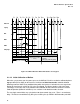
2.1.5 Dynamic Bus Inversion
In order to mitigate the effects of simultaneous switching outputs, AGP3.0 adopts a scheme called
Dynamic Bus Inversion (DBI) to limit the maximum number of simultaneous transitions on source
synchronous data transfers. DBI impacts only AD[31:0] and is used during source synchronous and
common clock transfers. Two new signals are defined to support DBI. DBI_LO and DBI_HI are used to
implement DBI on AD[15:0] and AD[31:16] respectively. The scheme used to implement DBI on source
synchronous transfers is as follows:
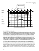
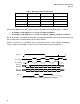
Whenever the number of bit transitions in AD[15:0] (or AD[31:16]) from one source synchronous period to
the next exceeds eight, the entire field is inverted by the transmitter in order to limit the maximum
transitions to eight. For example, if AD[15:0] changes from FF10 (hex) in source synchronous cycle A to
0000 (hex) in source synchronous cycle B, the DBI scheme is triggered in cycle B, thus inverting the
AD[15:0] to produce FFFF (hex). In this example, the number of transitions without DBI is nine, while with
DBI is seven. In order to signal to the receiver that the AD[15:0] are inverted in cycle B, DBI_LO will be
asserted high. The same scheme is used on AD[31:16]. DBI_HI is used to signal the inversion. The
receiver samples DBI_HI and DBI_LO to determine whether to invert AD[31:0] before using it.
Contiguous (back-to-back) DBI-enabled data transfers must continue the DBI encoding without break.
The only break that may occur in the DBI encoding happens when more than eight data bits are high in a
strobe group at the end of a transfer and transition low (terminating low, not driving) during the following
idle cycle. In this case there would be greater than 8 bits switching. This case can create more
switching noise. While there is sufficient time during the idle cycle for that noise to settle, the
system designer must be careful to avoid excessive crosstalk and reduced signal integrity on other
signals.
A similar scheme applies to common clock and Frame based (PCI) address and data transfers. In
these instances, DBI applies to transitions from one common clock period to the next.
Implementation of DBI is required in the transmitter and receiver for both the Master (graphics chip) and
the Target (core logic) when operating in 8X speed and in AGP V3.0 signaling mode. When doing Frame
based PCI transfers or 4X speed transfers in the same signaling mode, DBI is optional in the transmitter
but still required in the receiver.
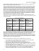
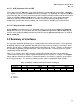
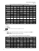
DBI is not supported when in AGP2.0 or AGP1.0 signaling modes. Table 8 illustrates the application of
DBI in various modes of operation.