
Accelerated Graphics Port Interface Specification

AGP3.0 Interface Specification
Rev. 1.0
51
3 AGP3.0 Physical Layer Specification
The AGP3.0 Physical Layer Specification defines a set of signaling levels, timing relationships and
topologies that support the enhanced performance capabilities of AGP3.0. The physical layer
specification provides for full backward compatibility with 1.5 V AGP2.0.
The purpose of this chapter is to set requirements for and make recommendations on DC and AC
specifications, maximum and minimum bus lengths, buffer characteristics and location of terminations.
The details are provided in the following subsections.
3.1 Overview
3.1.1 Introduction
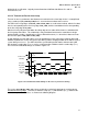
The AGP3.0 interface is designed to support several platform generations based upon 0.25µ (and
smaller) component silicon technology, spanning several technology generations. As with AGP2.0, the
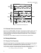
physical interface is designed to operate at a common clock frequency of 66 MHz. Its source
synchronous data strobe operation, however, is octal-clocked and transfers eight double words
(Dwords) of data within the span of time consumed by a single common clock cycle. The AGP3.0 data
bus provides a peak theoretical bandwidth of 2.1 GB/s (32 bits per transfer at 533 MT/s). Both the
common clock and source synchronous data strobe operation and protocols are similar to those
employed by AGP2.0.
11
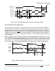
To accommodate the downward trend of V
CC
12
voltages brought about by continued process evolution
and the higher data transfer rates, AGP3.0 specifies a parallel-terminated bus with a fixed nominal
voltage swing of 800 mV peak-to-peak. To maintain compatibility with AGP2.0 topologies, the V
DDQ
connector pin remains as 1.5 V nominal.
AGP3.0 requires impedance compensation for signal integrity purposes. When the component’s I/O
interface is in “receive mode,” the integrated termination device
13
must have already been adjusted to
the appropriate impedance. The impedance of the AGP3.0 pull-up driver depends only on the driving
component’s V
DDQ
voltage and the impedance value of the termination; the pull-up driver impedance
should be set so that the proper output swing voltage is observed.
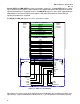
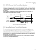
3.1.2 AGP3.0 Signal Definitions
AGP3.0 is a point-to-point interconnect that contains three types of signals. The two primary sets of
signals are the source synchronous signals for data transfer and common clock signals for arbitration
and control. The third type of signals (referred to as “asynchronous” in subsequent text) is not bound to
the AGP3.0 clocking schemes in any way whatsoever and pertains solely to out-of-band
communications. No other topology, beyond a point-to-point interface, is supported.
AGP3.0 specifies only four additional signals to the interface specification of AGP2.0: GC_DET#,
MB_DET#, DBI_HI, and DBI_LO.
11
See the AGP2.0 Interface Specification for detail.
12
The V
CC
voltage refers to the voltage that a given component uses to power its core logic.
13
The “integrated termination device” may very well include the AGP3.0 pull-down transistor, which also is used for driving
the bus when the component is in its drive mode of operation.