
Accelerated Graphics Port Interface Specification

AGP3.0 Interface Specification
Rev. 1.0
53
relationship from that of AGP2.0 (e.g. the SBA bits are now SBA#, indicating that a logic 1 is signaled as
a low voltage on the interconnect).
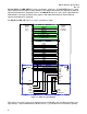
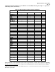
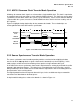
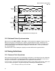
Table 30: AGP3.0 Signals and Associated Clock Domains
Signal Name Clock Domain
Source Synchronous Common Clock Asynchronous USB
**SBA#[7::0]
ü
**RBF
ü
**WBF
ü
ST[2::0]
ü
AD
_
STBF[1::0]
ü
AD
_
STBS[1::0]
ü
SB_STBF
ü
SB_STBS
ü
CLK
ü
USB+
ü
USB
-
ü
OVRCNT#
ü
PME#
ü
TYPEDET#
ü
GC_DET#
ü
MB_DET#
ü
**FRAME
ü
**IRDY
ü
**TRDY
ü
**STOP
ü
**DEVSEL
ü
**PERR
ü
**SERR
ü
**REQ
ü
**GNT
ü
RST#
ü
AD[31::0]
ü
ü
**C#/BE[3::0]
ü
ü
PAR
ü
INTA#, INTB#
ü
Vrefcg, Vrefgc
ü
DBI_HI, DBI_LO
ü ü
Signals marked as either Common Clock or Source Synchronous in Table 30 are capable of supporting
533 MT/s interface using a 800 mV swing referenced to ground and a 350 mV input reference voltage.
14
14
CLK is the single exception, as it is only a 66MHz signal clock. Its electrical characteristics remain unchanged from the
AGP interface specification.