
Accelerated Graphics Port Interface Specification
AGP3.0 Interface Specification
Rev. 1.0
54
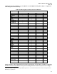
Collectively these signals are referred to as AGP3.0 signals because they share this same signaling
scheme. The remainder of this chapter is concerned primarily with this set of signals.
/ NOTE
In many cases, AGP3.0 signals have been defined as logically inverted from those of the
AGP2.0 Interface specification. This has been done to minimize power consumption, especially
in the quiescent state of the interconnect. This is more fully described in Section 2.1.
Further, note that the weak pull-up or pull-down resistance that is required for AGP2.0 signals
must not be present on the AGP3.0 channel or motherboard. Therefore, these resistances must
be integrated into the core logic device and electrically removed during AGP3.0 operation.
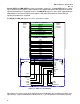
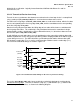
Electrically, GC_DET# is defined identically to the AGP TYPEDET# signal, a static signal either left
floating or pulled to ground by the AGP3.0 capable add-in card. The MB_DET# signal also is electrically
similar to TYPEDET#, however, it is either left floating or pulled to ground by the AGP3.0-capable
motherboard. GC_DET# and MB_ DET# are used to establish whether or not the channel is to be
operated in AGP3.0 or AGP2.0, 1.5V configuration. If TYPEDET# is open, the graphics card is indicating
that its capability is limited to AGP3.3V.
The Vrefcg connector pin is supplied by the motherboard (or core-logic) to provide AGP2.0 Vref or
AGP3.0 Vref to the graphics card based on the configuration detected. Likewise, the Vrefgc pin is
supplied by the Graphics Card to provide AGP2.0 or AGP3.0 Vref to the motherboard based on the
configuration detected. The connector signals TYPEDET#, GC_DET#, and MB_DET# are used to
establish the channel’s configuration. Refer to section “3.4.1.2) Vref Generation” for more detail.
INTA#, INTB#, and PME# are all 3.3 V “open drain” signals driven by the AGP Master, referenced to the
VCC3.3 power supply. These signals’ output buffers either need to be 3.3 V tolerant, or a solution
external to the component needs to be provided so that acceptable levels are maintained at the
interface.
CLK and RST# are also 3.3 V signals that may require that special controller input circuitry or dividers
be provided to prevent over-voltage or signal distortion at the pin.
USB signals are provided to support a Universal Serial Bus; the reader is directed to the USB
specification for further details.
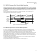
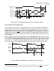
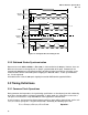
3.2 Transfer Mode Operations
A description of the principal in-band operating modes for AGP3.0 (the so-called “common clock” and
“source synchronous” transfer modes) is provided in the following section. Functional characteristics of
the AGP3.0 Transfer Modes are quite similar to those of AGP2.0 with all modifications guided by the
need to support the 8x data transfer rate of AGP3.0’s source synchronous mode.