
Accelerated Graphics Port Interface Specification

AGP3.0 Interface Specification
Rev. 1.0
56
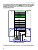
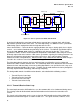
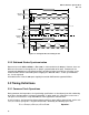
Figure 3-3: Source Synchronous Mode Time Domain
As previously indicated, the outer loops of both devices operate from a common clock, with all outer
loop controls specified relative to this clock. The inner loop timings use additional source synchronous
strobe timing signals employed to realize the high data transfer rates.
Source timed strobes -- where the device supplying the data also sources timing signals for use by the
receiver -- are used to null out data transport delays at the receiver. The AGP3.0 specification requires
that a pair of AD_STBF/AD_STBS strobes be supplied for each group of 16 data bits. These source
synchronous strobes are to be centered within the output data’s valid window, and used by the receiver
to directly capture data at the interface. With source synchronous signaling, the limiting parameter is no
longer the absolute time delay between transmitter and receiver, but is rather the delay matching
between the strobes and the data bits. Note that strobe usage is different than AGP2.0 (strobe usage is
covered in the section on Transmit to Receive Inner Loop).
The timing dependencies between the inner and outer loops are defined by a precise relationship
between the strobes and the common clock. This relationship allows for a deterministic transfer of data
between the inner and outer loops, where these timing dependencies are specified in such a way as to
allow implementation flexibility at the receiver. Tradeoffs may be made between the latency through the
inner loop, implementation technology, and/or design complexity.
This timing model contains four different time domains, to be detailed in the following sections:
• Transmit/Receive Outer Loop
• Transmit to Receive Inner loop
• Receive Inner to Outer Loop
• Transmit Outer to Inner Loop
3.2.2.1 Transmit/Receive Outer Loop
The outer loop between the AGP3.0 devices uses the common clock as its fundamental timing source.
These timings allow for bi-directional control of information transfer between the transmitter and
receiver.
The signals in this timing group are the same as those for AGP2.0 and have the timing relationships
defined for common clock signals as listed in Section 3.3.1. The signal electricals, however, are as
Outer Loop
Inner Loop
Transmitter
Receiver
Data
Timing
Control
data
timing
data
timing
66 MHz Clock