
Accelerated Graphics Port Interface Specification

AGP3.0 Interface Specification
Rev. 1.0
57
defined in this specification -- logically inverted from that of AGP2.0 with different V
OH
and V
OL
characteristics, etc.
3.2.2.2 Transmit to Receive Inner Loop
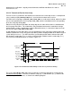
Transfer of source synchronous data between transmit and receive inner loop circuits is accomplished
using a strobe pair (AD_STBF/AD_STBS) that is sent from the transmitter to the receiver.
For AGP3.0, the rising edges of both AD_STBF and AD_STBS are used to transfer data, with the first data
transfer corresponding to the first rising edge of AD_STBF, and the second data transfer corresponding
to the first rising edge of AD_STBS.
Note that in many diagrams that follow, the falling edge of one strobe will be shown as coincident with
the rising edge of the other. This relationship is only coincidental and not to be counted on in design
implementations; strobes should not be used in a differential manner (i.e., do not base data transfer on
the crossover point of AD_STBF and AD_STBS).
As with AGP2.0, transmit strobe edges are to be positioned near the center of the minimum data valid
window, to provide the receiver the greatest possible input data sampling window for the widest range of
system timing skew cases. The AGP3.0 interface specification provides both a minimum data valid
time before the strobe edge (T
DVb
), as well as a minimum data valid time after the strobe edge (T
DVa
).
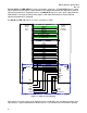
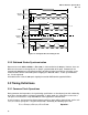
These transmit strobe/data timings are shown in Figure 3-4.
Transmit
AD_STBS
Transmit
Data
Data1 Data2 Data3
Transmit
AD_STBF
t
DVb
t
DVa
Data4 Data5 Data6 Data7Data0
t
TSf
t
TS8r
Common Clk
(66 MHz)
Figure 3-4: Transmit Strobe/Data Timing for 8X Source Synchronous Timing
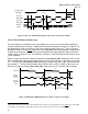
The receive AD_STBF/AD_STBS strobe inputs are directly used to latch data into the receiving device
based on their rising edges. Therefore, a minimum setup (t
RX_SU
) and hold time (t
RX_H
), relative to the
strobe, is required at the receiver, as shown in the following diagram: