
Accelerated Graphics Port Interface Specification
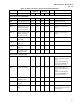

AGP3.0 Interface Specification
Rev. 1.0
83
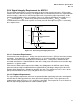
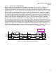
3.6.4 Signal Integrity Requirement for AGP3.0
The overshoot requirements are meant to protect the device from electrical overstress (EOS) and to
minimize the effects from ISI on timing. The ringback limits are intended to prevent false signal detection
and false strobes, and to insure sufficient input drive levels to guarantee proper input timing. On-die
clamping and ESD diode effects are included. Figure 3-16 shows the definition of overshoot (V
OSH_P
,
V
OSH_N
) and ringback (V
RB
). Note that any voltage excursion away from V
OL
and V
OH
, whether
associated with a transition on the signal or caused by crosstalk from adjacent signals, is covered by
these requirements.
V
REF
V
OH(Steady)
V
OL(Steady)
V
OSH_P
V
OSH_N
V
RB
V
RB
Figure 3-16: General Signal Integrity Waveform
3.6.4.1 Overshoot Requirements
Overshoot has two consequences: timing skew and electrical overstress (EOS) of transistor junctions
and oxides. Overshoot (V
OSH_P
) and undershoot (V
OSH_N
) are measured with respect to the steady-
state value of the driver after driving that level for three bit times. Timing skew is minimized if the
overshoot waveform has settled to within 0.2 volts of its steady-state value before the next strobe edge,
whether it is a signal or strobe.
EOS concerns limit the driver output level to Vddq, since Vddq powers the AGP3.0 signals. During
power-on and especially in motherboards that support AGP2.0, full voltage swing may be observed.
Negative buffer output level is limited to an absolute -0.3 volts. This voltage level causes stress to the
pull-up transistor drain-to-source (V
DS
) and gate-to-source (V
GS
) voltages.
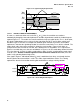
3.6.4.2 Ringback Requirements
The signal integrity requirements have been augmented to allow significantly more noise and ringback
after the data or strobe input buffer has been given time to properly switch. If the signal enters the
shaded region shown in Figure 3-17, it is treated as a transition. Crossing the DC V
IL
or V
IH
limits has
different signal integrity implications for strobe and data signals.