
Accelerated Graphics Port Interface Specification

AGP3.0 Interface Specification
Rev. 1.0
85
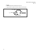
3.6.4.2.2 SPECIAL GAD SI REQUIREMENTS
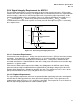
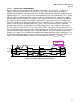
There are two cases for GAD signals: full transitions and glitches. In the first case, as soon as an
Address or Data signal transitions across the DC V
IL
or V
IH
limits, the transition must continue
monotonically through the VREF switch point to V
RB
overdrive beyond VREF, outside the shaded keep-out
region of Figure 3-17. The GAD signals must remain outside the keep-out region for time T
DRIVE
. At this
point, the signal is allowed more noise as long as it does not violate the DC V
IL
and V
IH
limits until the
next transition, with one exception (see Figure 3-19c). Figure 3-19a shows an example of an allowed
GAD signal shelf that exceeds the V
RB
overdrive requirement. Figure 3-19b shows an example of GAD
noise that exceeds the V
RB
limit, but is allowed since it is beyond the T
DRIVE
requirement. Figure 3-19c
shows a set of GAD signals that glitch above the V
IL
(max). The case where the signal is high and
glitching below V
IH
(min) is assumed to be the same by complement. If the signal exceeds V
IL
(max),
then the signal must settle for T
DRIVE
, just as for a full transition. If the signal exceeds VREF, then T
DRIVE
is measured from the last crossing of VREF. If the signal does not exceed VREF, then T
DRIVE
is measured
from the peak of the glitch. While this case is allowed, it indicates excessive crosstalk or other signal
integrity issues and its cause should be investigated and avoided if possible. Figure 3-19d shows a set
of GAD signals that glitch below the V
IH
(min), but the next transition of the GAD signal occurs before T
DRIVE
expires. This is a timing violation. In all cases, the GAD signals must meet T
RX_SU
and T
RX_H.
Figure 3-19: Address/Data Ringback Examples
V
RB
V
IH
(min)
T
DRIVE
V
IL
(max
V
REF
V
REF
T
DRIVE
V
RB
B
A
C
D
T
DRIVE
Violations