
Accelerated Graphics Port Interface Specification

AGP3.0 Interface Specification
Rev. 1.0
86
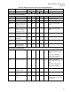
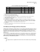
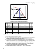
Table 42: Input/Output Signal Integrity Requirements
Symbol Parameter Min Max Units Notes
Output Slew Rate 2 3.5 V/ns 1,2,3
Input Slew Rate 1 3.5 V/ns 7
V
OSH_P
Positive overshoot above
steady level 350 mV 1,4,8
V
OSH_N
Negative overshoot below steady level -300 mV 1,4,8
V
RB
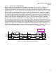
Ringback margin to Vref 150 mV 1,5
T
DRIVE
Input overdrive time 0.6 ns 6
1. Output buffer measurements are made with a standard 50 Ω load to ground (see Table 39). Input
measurements are specified at the die pad.
2. Slew rate is measured at the driver’s output pad.
3. For system designs requiring a minimum of EMI it is recommended that the output slew rate be held as
close to the minimum as possible.
4. Steady High (Low) voltage level is defined as a voltage High (Low) level after 3 (three) Bit times.
5. See Table 39 for V
REF
definition.
6. The ringback spec is defined in order to guarantee a window of an extra 50mV around the V
IH
and V
IL
spec.
That is, the ringback must be small enough so that the signal does not ring back to ±150mV of the reference
voltage. This also applies to edge non-monotonicities such as ledging. V
RB
defines a keep-out zone in which
the signal shall not transgress except during transitions and before T
DRIVE
.
7. See Table 41.
8. Timing skew is minimized if the overshoot waveform has settled to within 0.2 volts of its steady-state value
before the next strobe edge
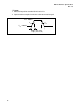
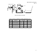
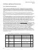
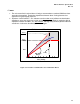
3.6.5 Maximum AC Ratings and Device Protection
All AGP3.0 input, bi-directional, and output buffers must be capable of withstanding continuous exposure
to a waveform such as that shown in Figure 3-20. It is recommended that these waveforms be used as
qualification criteria against which the long-term reliability of each device is evaluated. This level of
robustness must be guaranteed by design; however, it is not intended that this waveform be used as a
production test.
These waveforms are applied with the equivalent of a zero impedance voltage source, driving through a
series resistor directly into each AGP3.0 input or tri-stated output pin. The open-circuit voltage (of the
voltage source is shown in Table 43) is based on the expected worst-case overshoot and undershoot
that is expected in actual AGP3.0 interconnects.
/ NOTE
The voltage waveform is supplied at the resistor shown in the evaluation setup, not the package
pin.