
Accelerated Graphics Port Interface Specification

AGP3.0 Interface Specification
Rev. 1.0
91
3.6.6.2 Signal swing (V
OH
) Accuracy
Signal timing characteristics and quality are highly dependent on the signal swing values observed at the
receiver. In general, V
OH
represents the voltage attained at the receiver input as the signal settles.
Designs are expected to maintain V
OH
at least above 750 mV at V
DDQ
= 1.5 volts, and preferably near the
Vswing target value of 800 mV but below 850mV. Signal swing values that are too large may result in
unacceptable levels of overshoot, ringback, or settling time.
3.6.6.3 Receiver Characteristics
A differential input receiver is essential for AGP3.0 operations. The voltage reference is specified to be
0.350 V at a nominal V
DDQ
value. This reference voltage may be generated locally from V
DDQ
. To
reduce the current consumption of the V
REF
supply, the differential input buffer must be designed with
low input leakage current. The combined load on either Vrefcg or Vrefgc of all inputs must be less than
50 µA.
The receiver should be designed to handle input swings as little as 250mV to 450mV.
Furthermore, buffer V/I characteristics outlined above are primarily to ensure a proper receiver
termination, although they also apply to the driver pull-down.
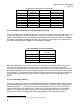
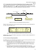
3.6.6.4 Input Switching
The differential input buffer must be designed to have sufficient gain to convert a small differential input
voltage to a full internal CMOS voltage swing without introducing additional skews. Timing analysis
indicates that the variance in switch point voltage must be relatively tight for a given signal group.
Switch point voltage is the voltage at which the receiver determines that the input is switching from a
one to a zero or vice-versa. Part-to-part and inter-group variations are more relaxed than intra-group
variations and are listed in Table 46.
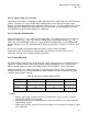
Table 46: Part-to-part and Intra-group Variations
Grouping Margin Window Units Notes
Intra-group
± 30 mV 1
Inter-group
± 100 mV 2, 3
Part-to-part
± 100 mV 2.3
/ NOTE
1. Within a signal group, all data receivers must switch within ± 30 mV of their associated
strobe being sensed on its rising edge.
2. Inter-group and part-to-part requirements are such that all receivers must switch within the
range of Vref ± 100mV.
3. Switch point variations must take into account variations in the external Vref reference signal
due to all effects.