
Audio Codec '97

AC ‘97 Component Specification Revision 2.3 Rev 1.0
101
Rise and Fall times, flight times, Output Valid Delay, Input Setup and Hold, and worst case capacitive loads (see
Section 9.2.7) should be used together for modeling of the AC-link output pin drivers.
For example, the following worst case scenario situates the Primary Codec along with a Secondary Codec on a riser
15 inches from the Controller. The AC-link BIT_CLK, SYNC, and SDATA_OUT signals are loaded with ~55 pF
external capacitance. The Primary drives BIT_CLK to the Controller with a 7 ns combined rise plus flight time, the
Controller delays 15 ns in driving SDATA_OUT valid (includes the 7 ns return combined rise or fall plus flight
time), and the Codec requires stable data 10 ns prior to latching. Assuming the minimum BIT_CLK high time of 36
ns (provided by the new 45/55 duty cycle requirement) yields:
36 – ( 7 + 15 + 10) = 4 ns margin
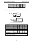
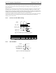
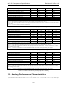
9.2.4 Signal Rise and Fall Times
Figure 34. Signal Rise and Fall Timing Diagram
Parameter Symbol Min Typ Max Units
BIT_CLK rise time (Note 1) Trise
clk
- - 6 ns
BIT_CLK fall time (Note 1) Tfall
clk
- - 6 ns
SYNC rise time (Note 2) Trise
sync
- - 6 ns
SYNC fall time (Note 2) Tfall
sync
- - 6 ns
SDATA_IN rise time (Note 3) Trise
din
- - 6 ns
SDATA_IN fall time (Note 3) Tfall
din
- - 6 ns
SDATA_OUT rise time (Note 2) Trise
dout
- - 6 ns
SDATA_OUT fall time (Note 2) Tfall
dout
- - 6 ns
Note 1: BIT_CLK rise/fall times with an external load of 75 pF
Note 2: SYNC and SDATA_OUT rise/fall times with a external load of 75 pF
Note 3: SDATA_IN rise/fall times with an external load of 60 pF
Note 4: Rise is from 10% to 90% of Vdd (V
ol
to V
oh
)
Note 5: Fall is from 90% to 10% of Vdd (V
oh
to V
ol
)
Table 59. Signal Rise and Fall Time Parameters