
Audio Codec '97

AC ‘97 Component Specification Revision 2.3 Rev 1.0
102
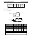
AC ‘97 2.3 maintains the original specified BIT_CLK, SYNC, SDATA_OUT, and SDATA_IN signal rise and fall
times. These signals must also meet the Output Valid Delay time with respect to the rising edge of BIT_CLK
specified in Table 56.
Modeling of the AC-link output pin drivers should include rise and fall times, flight times, and external capacitive
and inductive loads, which could be as large as 75 pF. Special consideration should be given to the BIT_CLK
output pin driver for any Primary Codec that is designed to operate in multiple Codec and/or riser implementations.
In addition, the same consideration should be given to SYNC and SDATA_OUT output pin drivers for any AC ‘97
Controller that is designed to operate in multiple Codec and/or riser implementations.
System designers should be aware that with the increased driver strengths required to meet the above rise/fall times
(with specified load), point-to-point routings with low total capacitive loads might require EMI reduction
techniques, such as series resistors.
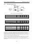
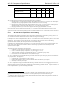
9.2.5 AC-link Low Power Mode Timing
Figure 35. AC-link low power mode timing diagram
Parameter Symbol Min Typ Max Units
End of Slot 2 to BIT_CLK,
SDATA_IN low
Ts2_pdown - - 1.0 µs
Table 60. AC-link low power mode timing parameters
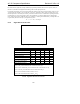
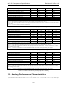
9.2.6 ATE Test Mode
Hi-Z
SDATA_OUT
T
off
RESET#
T
setup2rst
SDATA_IN, BIT_CLK,
EAPD, SPDIF_OUT,
and DIGITAL I/O
Figure 36. ATE test mode timing diagram
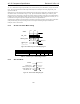
Data
PR4
Note:
BIT_CLK not to scale
Slot 1 Slot 2
SDATA_IN
SDATA_OUT
BIT_CLK
SYNC
T
s2_pdown
Write to
0x26