
Audio Codec '97

AC ‘97 Component Specification Revision 2.3 Rev 1.0
103
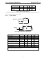
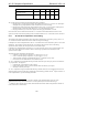
Parameter Symbol Min Typ Max Units
Setup to trailing edge of RESET#
(also applies to SYNC)
Tsetup2rst 15.0 - - ns
Rising edge of RESET# to Hi-Z delay Toff - - 25.0 ns
Table 61. ATE test mode timing parameters
All AC-link signals are normally low through the trailing edge of RESET#.
1.
Bringing SDATA_OUT high for the trailing edge of RESET# causes an AC ’97 Codec’s AC-link outputs
and Digital I/O to go high impedance which is suitable for ATE in circuit testing.
2.
Bringing SYNC high for the trailing edge of RESET# causes an AC ’97 Codec to enter a vendor-specific
internal test mode. This mode has no effect on AC ‘97 AC-link output signal levels.
3.
Bringing both SDATA_OUT and SYNC high for the trailing edge of RESET# is reserved.
Once either of the two test modes has been entered, AC ‘97 must be issued another RESET# with all AC-link
signals low to return to the normal operating mode. For additional details on AC ’97 test modes, refer to Section 8.1.
9.2.7 AC-link IO Pin Capacitance and Loading
The utilization and popularity of multiple Codec configurations and OEM riser card audio is growing, and AC ‘97
2.3 Controllers and Codecs intended for such uses need to be designed accordingly.
In multiple Codec and riser implementations, the AC ‘97 Controller drives SYNC and SDATA_OUT to two or more
destinations. The Controller’s SYNC and SDATA_OUT output pin drivers need to meet AC-link timing
requirements when loaded by the total capacitance on each of these outputs.
In multiple Codec implementations, the Primary AC ‘97 Codec drives BIT_CLK to two or more destinations. The
Codec’s BIT_CLK output pin driver needs to meet AC-link timing requirements when loaded by the total
capacitance on this output.
The following factors contribute to total capacitance:
• Controller or Codec output pin capacitance (7.5 pF max per AC ‘97 2.3)
• Codec or Controller input pin capacitance (7.5 pF max per AC ‘97 2.3)
• Total trace length capacitance on motherboard plus riser
19
(estimated 2.5 pF per inch)
• IO connectors, such as motherboard to riser (estimated 2.5 pF)
AC ‘97 2.3 compliance requires that the following Controller and Codec
input and output pins have a maximum of
7.5 pF capacitance. This applies to:
• Controller BIT_CLK and SDATA_IN[0-3] inputs
• Primary and Secondary Codec, as well as Controller SYNC and SDATA_OUT inputs
• Secondary Codec BIT_CLK input
AC ‘97 2.3 compliance strongly recommends the following Controller and Codec AC-link output pin drivers be of
sufficient strength to meet AC-link timing requirements for the following specified external
20
capacitive loads in 1-4
Codec implementations, as per the following three tables:
19
Motherboard plus riser trace lengths, especially in multiple Codec implementations such as AC down
(motherboard) and MC up (riser), could exceed ~15 inches, particularly in NLX form factor designs.
20
In addition to these external capacitive loads, additional allowance must be made for the particular Controller or
Codec (internal device characteristic).