
Audio Codec '97

AC ‘97 Component Specification Revision 2.3 Rev 1.0
6
6.7.1 ADC Loopback '001'............................................................................................................................86
6.7.2 Local analog Loopback '010'...............................................................................................................86
6.7.3 DAC Loopback '011'............................................................................................................................86
6.7.4 Remote analog Loopback '100'............................................................................................................86
7. Power Management...........................................................................................................................................87
7.1 POWER MANAGEMENT “D STATE” MAPPINGS FOR AUDIO CODECS .............................................................88
7.2 POWER MANAGEMENT “D STATE” MAPPINGS FOR MODEM CODECS...........................................................88
7.3 POWER MANAGEMENT WITH WAKE-UP CAPABILITIES .................................................................................89
7.3.1 Primary MC’97 Codec and MLNK......................................................................................................89
7.3.2 Secondary MC’97 Codec and MLNK ..................................................................................................90
7.4 WARM AND COLD AC-LINK RESET CONSIDERATIONS .................................................................................90
7.4.1 Resume Reset Behavior........................................................................................................................90
7.4.2 Resuming Normal AC-link Operation from S3, S4 or S5 System Sleep State ......................................92
7.4.2.1 AC-link RESET# SIGNALING REQUIREMENT.......................................................................................... 92
7.5 POWER DISTRIBUTION..................................................................................................................................93
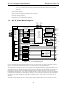
7.5.1 MC ‘97 (Primary) Implementations.....................................................................................................93
7.5.2 AC ‘97 (Primary) + MC ‘97 (Secondary) Implementations ................................................................94
7.5.3 AMC ‘97 (Primary) Implementations ..................................................................................................95
7.6 AC + MC CLOCKING CONSIDERATIONS ........................................................................................................95
7.7 RESUME LATENCY: DEVICE DRIVER CONSIDERATIONS ...............................................................................95
8. Testability ...........................................................................................................................................................96
8.1 ACTIVATING THE TEST MODES.....................................................................................................................96
8.2 TEST MODE FUNCTIONS ...............................................................................................................................96
8.2.1 ATE in circuit test mode.......................................................................................................................96
8.2.2 Vendor-specific test mode....................................................................................................................96
9. Digital DC and AC Characteristics..................................................................................................................97
9.1 DC CHARACTERISTICS .................................................................................................................................97
9.2 AC TIMING CHARACTERISTICS.....................................................................................................................97
9.2.1 Reset Timing ........................................................................................................................................97
9.2.1.1 Recommended AC-link Cold Reset Behavior and Timing............................................................................... 97
9.2.1.2 Warm Reset Timing ......................................................................................................................................... 98
9.2.2 AC-link Clocks.....................................................................................................................................99
9.2.3 Data Output and Input Times ............................................................................................................100
9.2.4 Signal Rise and Fall Times ................................................................................................................101
9.2.5 AC-link Low Power Mode Timing .....................................................................................................102
9.2.6 ATE Test Mode ..................................................................................................................................102
9.2.7 AC-link IO Pin Capacitance and Loading.........................................................................................103
10. Analog Performance Characteristics .........................................................................................................104
Appendix A. AC ‘97 Register Set Summary .........................................................................................................106