
Audio Codec '97

AC ‘97 Component Specification Revision 2.3 Rev 1.0
7
LIST OF FIGURES
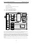
Figure 1. AC ‘97 Codec Block Diagram ...................................................................................................................10
Figure 2. AC ‘97 System Diagram ............................................................................................................................11
Figure 3. AC ‘97 48-pin package and pinout.............................................................................................................13
Figure 4. AC ‘97 48-pin package dimensions ...........................................................................................................14
Figure 5. Example of vendor-independent external capacitor layout connection......................................................18
Figure 6. Controller to Codec connections ................................................................................................................19
Figure 7. Codec Clock Source Detection....................................................................................................................20
Figure 8. Controller to Multiple Codec connections..................................................................................................21
Figure 9. AC-link Powerdown Timing ......................................................................................................................24
Figure 10. Bi-directional AC-link Frame with Slot assignments...............................................................................26
Figure 11. AC-link Output Frame ..............................................................................................................................29
Figure 12. Start of an AC-link Output Frame.............................................................................................................30
Figure 13. AC-link Input Frame .................................................................................................................................33
Figure 14. Start of an AC-link Input Frame................................................................................................................33
Figure 15. Audio I/O ..................................................................................................................................................38
Figure 16. Primary Codec Multichannel implementation...........................................................................................40
Figure 17. AC ‘97 Mixer Functional Diagram ...........................................................................................................43
Figure 18. AC-link Slot Definitions ...........................................................................................................................45
Figure 19. AC-link Slot Assignments.........................................................................................................................73
Figure 20. “Conceptual” Example of GPIO Pin Implementation...............................................................................75
Figure 21. Combined Audio / Modem AFE Auxiliary Power Distribution................................................................77
Figure 22. AC-link Low Power Mode........................................................................................................................78
Figure 23. AC-link Warm Reset.................................................................................................................................78
Figure 24. AC-link Power-down/Up Sequence ..........................................................................................................78
Figure 25. Split Partitioned Design Example .............................................................................................................79
Figure 26. Loopback points .........................................................................................................................................86
Figure 27. One example of AC ‘97 Powerdown/Powerup flow .................................................................................87
Figure 28. AC ‘97 Powerdown/Powerup flow with analog mixer still alive.............................................................87
Figure 29. Cold Reset timing diagram when the codec is supplying the BIT_CLK signal ........................................98
Figure 30 Cold Reset timing diagram when BIT_CLK is being provided by an external source...............................98
Figure 31. Warm Reset timing diagram.......................................................................................................................98
Figure 32. BIT_CLK and SYNC Timing diagram .....................................................................................................99
Figure 33. Data Output and Input Timing Diagram ..................................................................................................100
Figure 34. Signal Rise and Fall Timing Diagram .....................................................................................................101
Figure 35. AC-link low power mode timing diagram................................................................................................102
Figure 36. ATE test mode timing diagram ................................................................................................................102
LIST OF TABLES
Table 1. AC ‘97 48-pin package pinlist.....................................................................................................................14
Table 2. Power Signal Descriptions...........................................................................................................................15
Table 3. AC-link and Clocking Signal Descriptions..................................................................................................15
Table 4. Digital I/O Signal Descriptions ...................................................................................................................16
Table 5. Analog I/O Signal List.................................................................................................................................17
Table 6. Filtering and Voltage Reference Signal List................................................................................................18
Table 7. Recommended Codec ID strapping .............................................................................................................22
Table 8. VRA Behavior.............................................................................................................................................28
Table 9. Output Slot 0 Bit Definitions.......................................................................................................................30
Table 10. Input Slot 1 Bit Definitions.........................................................................................................................34
Table 11. Primary Codec Addressing: Slot 0 Tag Bits...............................................................................................37
Table 12. Secondary Codec Addressing: Slot 0 tag bits .............................................................................................37
Table 13. Default Slot to DAC Mappings Based on Codec ID ..................................................................................41
Table 14. Audio Slot Data Definitions .......................................................................................................................46
Table 15. Audio Interrupt Slot Definitions .................................................................................................................46