
Audio Codec '97

AC ‘97 Component Specification Revision 2.3 Rev 1.0
74
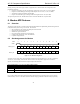
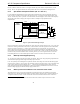
performing a read operation over the link. Table 40 describes the GPIO output and input slot assignments.
Input and Output Slot 12: GPIO Pin Status and Control
Bit Description
19-4 GPIO Pin Status (see Table 41. Recommended Slot 12 GPIO Bit Definitions)
3-1 Vendor specific
0 GPIO_INT mask enabled input pin event interrupt (1=event) (input Slot 12 only)
Table 40. Slot 12-Bit Definitions
6.3 GPIO Pin Definitions
General Purpose Input/Output (GPIO) pins are programmable to have input/output functionality. The data values
(status) for these pins are all in one register, with input/output configuration in a separate register. Control of GPIO
pins configured for output is achieved by setting the corresponding bit in output slot 12; status of GPIO pins
configured for input is returned on input slot 12. The Codec must constantly set the GPIO pins that are configured
for output, based upon the value of the corresponding bit position of the control slot 12. The Codec should ignore
output slot 12 bits that correspond to GPIO control pins configured as inputs. The Codec must constantly update
status on input slot 12, based upon the logic level detected at each GPIO pin configured for input. A GPIO output
pin value that is written via slot 12 in the current frame won’t affect the GPIO status that is returned in that
particular write frame.
This slot 12-based control/status protocol minimizes the latency and complexity, especially for host-based
Controllers and host data pump software, and provides high speed monitoring and control, above what could be
achieved with command/status slots. For host-based implementations most AC ‘97 registers can be shadowed by
the driver in order to provide immediate response when read by the processor, and GPIO pins configured as inputs
should be capable of triggering an interrupt upon a change of status.
The AC-link request for GPIO pin status is always delayed by at least one frame time. Read-Modify-Writes across
the AC-link will thus incur latency issues and must be accounted for by the software driver or AC ‘97 Digital
Controller firmware. PCI retries should be kept to a minimum wherever possible.
6.3.1 GPIO Pin Implementation
The modem AFE contains a number of General Purpose Input/Output pins suitable for easy connection with
minimal parts to a DAA circuit. There is no requirement that a GPIO, when configured as output, must be able to
directly drive a relay coil. The AC ‘97 Digital Controller is responsible for configuring any GPIOs as outputs on
power-up, in order to drive transistors appropriately for DAA control.
When configured as an input, a GPIO must function as a CMOS Schmitt-triggered input for a 3.3V power supply.
To conserve power internal pull-ups or pull-downs should not be present. The board designers are responsible for
connecting unused pins to DVdd or DVss (or unconnected depending on manufacturer’s recommendations).
The GPIOs should be tri-stated to a high impedance state on power-on or a cold reset. It is up to the AC ‘97 Digital
Controller to first enable the output after setting it to the desired state. To prevent overdrive of any transistors, the
outputs should have slow rise and fall times. Typical values should be 40 nsec for 10% to 90% of DVdd with a 50
pF load. In addition, the device must sink 2-4 mA at a maximum level of 0.4 V and must source 2-4 mA at a
minimum level of 2.4 V.